Originally published by Antmicro
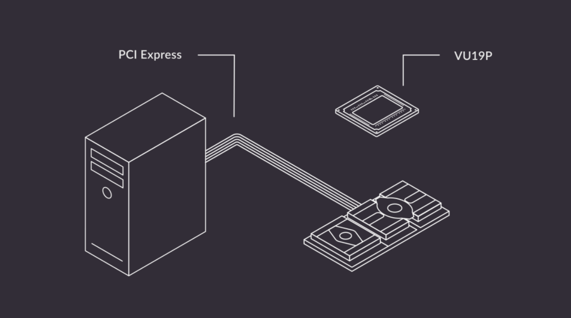
In the daily work at Antmicro, they use FPGAs primarily for their flexibility and parallel data processing capabilities that make them remarkably effective in advanced vision and audio processing systems involving high-speed interfaces such as PCI Express, USB, Ethernet, HDMI, SDI etc. that they develop and integrate as open source, portable building blocks. Many of their customers, however, use FPGAs also in a different context, namely for designing ASICs, which is a highly specialized market that typically involves large FPGAs, proprietary flows and IP. In one such project, Antmicro was working with one of the largest FPGAs in production today, the 9-million LUT Xilinx VU19. Being a design with considerable complexity, it needed a high-throughput link between the FPGA and the host PC that could be thoroughly benchmarked, analyzed and optimized for the use case.
Implementing PCIe with open source
Implementing PCIe is not completely straightforward as you have to synchronize multiple lines of high-speed bi-directional data. If you hit a bug somewhere in your data flow, things get very tricky to debug, especially if you have no ability to inspect and change the source code of the IPs involved. Being active developers of a variety of portable and reusable open source FPGA IP cores, for the project in question Antmicro was able to integrate a fully open PCIe interface into the Xilinx VU19-based ASIC prototyping platform using LiteX/LitePCIe, achieving a pretty respectable throughput of 31 Gbits/s on an 8-lane bandwidth. Although the FPGA chip itself is capable of 16-lane bandwidth for transferring data, the proFPGA board used in the setup supports only 8 lanes, but with hardware capable of bigger bandwidth they can achieve even greater throughput if needed. In fact, the repository also contains instructions for a 16-lane capable VU9-based setup – using a popular and not as prohibitively expensive devboard available from after-market- where they could measure as much as 59 Gbits/s.

Scalable, portable and customizable flows
Antmicro’s ability to rapidly iterate as well as track down and fix bugs in the system they created for this customer project demonstrates the scalability and portability of the open source-based approach, and is an example of Antmicro’s wider efforts aimed at developing reusable building blocks and introducing improvements to the whole FPGA ecosystem.
Open source-licensed IP cores play well with the open source FPGA and ASIC tooling that we are building to enable a faster, collaborative and modular system development workflow – a goal that is shared by CHIPS Alliance, of which we are proud to be a Platinum member. As one of the many examples, Antmicro is making great progress in enabling open source synthesis and simulation of complex SystemVerilog-based designs, such as security-focused RISC-V cores like OpenTitan’s Ibex. Some of their other projects focus on open source synthesis and place & route flows, linters, formatters, CI systems, simulation platforms, test suites and more.
Flexible system design
The PCIe core used in the ASIC prototyping project also works great in sophisticated computer systems they have been building for our customers. The wide array of customizable and licence-free FPGA IPs and SoC generators that Antmicro works with allows them to implement specific functionalities in the devices they build and it includes MIPI CSI and other camera interfaces, SDI, HDMI, ISP processing, video codecs, AI and 2D GPU acceleration, I2S, SPDIF, PCIe, USB, Ethernet, DMA, SATA and DRAM controllers.
Antmicro’s customers have full control over the solutions built for them thanks to the open and vendor-neutral nature of the solutions Antmicro works with. If you are looking to build an FPGA or ASIC system that you truly own and understand, make sure to get in touch with them at contact@antmicro.com to hire their development services.