
Overview
This white paper describes how low-power memory technology, originally designed for large, high density, SRAMs has been enhanced and adapted to deliver low-power, low-voltage register files.
Introduction
There is a large, and growing, class of applications for which power is a critical factor, sometimes as a result of a desire to add increased functionality to already power-constrained devices, and in some cases where on-chip SRAM gives the most power efficient implementations. For example:
- Body-worn devices (“Wearables” – smart watches, fitness trackers, hearing aids, earbuds) with constrained form factors that limit battery size
- IoT devices with added AI features (security cameras with image recognition capability, voice-enabled devices), where the desire is to add functionality while maintaining long battery life
- AI devices where having large amounts of SRAM on chip is a requirement to enable high speed inferencing
Modern System-on-Chip (SoC) devices to address these applications have a hierarchy of data storage elements within them, such as:
- Single registers, embedded within processing logic, used for such tasks as holding control values, and pipelining the logic to improve processing speed.
- Register files – small memories that are closely coupled to blocks of logic. Register files are used for tasks such as temporary storage, buffering between blocks of logic, and data reordering, and are often required to make multiple accesses per clock cycle. An application will typically contain multiple independent register files, all operating simultaneously.
- SRAM – large memories that are more loosely coupled to the logic, and that hold less frequently used data. On-chip SRAM is commonly optimised for storage density, and limited to one access per memory instance per clock cycle. Often the memory instances are clustered together to create larger memory banks, but those larger banks are still limited to a small number of accesses per cycle.[1]
This white paper discusses how low-power SRAM technology can be adapted to deliver low-power register files.
[1] This classification of storage hierarchy is focused on underlying technology rather than system-level function. It views (for instance) a level 1 cache and a level 2 cache as similar examples of on-chip SRAM based on capacity and numbers of accesses per cycle, rather than seeing them as different entities because of their different functions in the overall system.
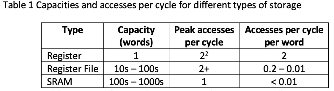
The differences between the storage levels listed above can be quantified by considering the capacity (i.e. number of different values stored simultaneously) and the number of accesses (reads or writes) per cycle, leading to an overall accesses per cycle per word metric, as shown in Table 1.
[1] i.e. 1 input and 1 output per cycle – the register can be both used and updated simultaneously
From this table, register files are closer to SRAM than to registers, but are distinguished from SRAM by having a smaller capacity (although there is some overlap between large register files and small SRAMs), and especially by providing more simultaneous accesses per cycle. Register file designs are therefore optimised for small capacity and rapid access (or multiple accesses per cycle), with the high storage density that is typical for SRAMs being of secondary consideration.
Standard Register File Architecture
Register files have traditionally been designed for performance and area, rather than low power operation. This means using foundry-supplied bit cells, that have been optimised for a combination of read current and area. The bit cell is combined with fast acting, but often power-hungry, peripheral circuits for reads and writes in order to provide high speed access to the stored data. This results in a design that is good for high-performance applications, but inappropriate for the kinds of power-constrained applications mentioned above. For those, a register file designed for low power is required.
Goals For A Power-Efficient Register File
The design goals for a power-efficient register file are different to those for a low-power SRAM. An important point is that a register file is physically smaller than an SRAM instance, and is more closely coupled to the SoC logic. This makes it necessary to consider not just how to save power in the register file itself, but also how the register file fits with the power saving strategy for the system logic.
Given that voltage scaling is a common technique for power reduction in logic, it follows that a register file should be able to integrate with logic using such a technique, without requiring separate supply rails and level shifters that simply add to overall system complexity. However, simply applying voltage scaling to the register file itself is not sufficient to reduce register file power, as explained in the next section.
Limits On Low-Voltage Operation Of A Register File
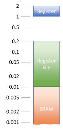
The ability of a memory (SRAM or register file) to operate at reduced voltage is normally limited by the bit cell – the basic data storage element (see Figure 1). Especially in the case of the 6T bit cell that is used in SRAM, the trade-offs made in the bit cell in order to enable it to reliably store data, to be read from, and to be written to, usually result in there being a limited voltage range over which the bit cell will operate. There are two basic ways to extend the operating range to enable low-voltage operation:
- Redesign the bit cell to improve functionality at low voltage, which results in bit cell area increasing, or
- Include read assist and write assist circuits in the overall memory design. These circuits boost the internal voltages used within the memory back to the range where the bit cell operates reliably, at the expense of increased circuit complexity and increased power dissipation.
To expand on the second point – if voltages are boosted within the register file, then the effective supply voltage for large parts of the register file is the boosted voltage rather than the external supply voltage. Power dissipation for these parts of the register file therefore depends on the boosted voltage (which is constrained to the operating voltage range of the bit cell) and does not reduce as expected if the external supply voltage is reduced.
To address this issue sureCore adopted the first option for the bit cell – redesigning it to improve functionality at low voltage, at the expense of area. We have chosen a design with separate read ports and write ports, that allows the read and write operations to be optimised separately without a need to compromise between the two functions and with no need for read or write assist. The bit cell has a modular design where we can easily add extra ports to the bit cell in order to add extra ports to the register file itself. SureCore’s experience of SRAM verification, using both Monte Carlo and High-Sigma Monte Carlo (HSMC) simulation to prove robust circuit operation over temperature, voltage and statistical process extremes has been applied to the bit cell. It has been evaluated on multiple CMOS processes, both bulk and FinFET, in order to demonstrate process portability of the cell, and both the circuit design and the physical floorplan have been shown to be portable.
For more details of sureCore’s verification methodology click here.
Low-Power Register File Architecture
The SureCore register file builds on the low-voltage bit cell described above, using similar circuit techniques to those used in our low-power SRAMs. These include:[1]
- Hierarchical partitioning of long wires with high capacitance, such as bit lines. Partitioning of these wires reduces the active capacitance, and therefore reduces active power and increases operating speed.
- Wide pre-decoding of addresses and structuring the control circuits in order to minimise activity on long wires.
- Use of our patented ‘Cascode Pre-charge Sense’ circuits that reduce bit line voltage swing, and thereby reduce both active and leakage power.
These are then supplemented by some register file specific techniques. In particular, the use of separate read and write ports on the bit cell means that there are separate read and write bit lines, and therefore there is no need for a shared bit line to be initialised to a common starting state for all accesses. Instead, it is possible to set the states of read and write bit lines separately:
- The write bit lines use a Non-Return-to-Zero (NRZ) implementation, where the bit line retains its state from one write cycle until the data arrives for the next write. This reduces the number of transitions on the write bit lines, and therefore reduces write power.
- The read bit line uses a targeted just-in-time pre-charge scheme, where the pre-charge circuit and the column multiplexer are combined so that only the bit lines that are required for the read cycle are pre-charged and then selectively discharged by the selected bit cells. Again, this reduces the number of bit line transitions, and therefore reduces power.
[1] There is a separate SureCore white paper that describes our low-power SRAM technology, available here
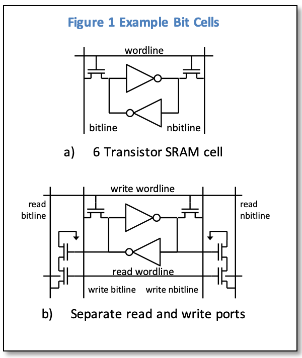
Figure 2 Shows a block diagram of the register file, annotated with the additions made in order to reduce power. As can be seen, there are changes throughout the design that all contribute to the overall power reduction.
Figure 2 Block Diagram Of Register File, Showing Power Reduction Technologies
Benchmarking
Third party benchmarking has indicated that sureCore register files can deliver very significant power savings compared to more traditional register file designs. In particular dynamic power savings in the region of 75% can be shown. Furthermore, the capability to operate over a wide voltage range means that both typical and low power operating modes of an SoC may be optimised.
Summary
This paper explains how sureCore’s specialised low-power register file design is optimised to achieve both low operating voltage and low power consumption. This architecture significantly eases integration with low voltage on-chip. This was achieved by:
- Using a custom bit cell, with separately optimised read and write ports, that is designed to work at low voltage,
- Using our existing low-power SRAM design techniques to reduce active power in the periphery circuits, and
- Adding additional register file specific optimisations to further reduce activity on the register file bit lines.
For many applications cutting power is the #1 priority – even often at the expense of area. In these cases, reviewing the contribution made to overall consumption by register files can be an illuminating analysis. The sureCore low power register file provides a welcome addition to the system designers battle to reduce power.
About sureCore
sureCore is a supplier of low-power and low-voltage SRAM IP. Our EverOn and PowerMiser SRAM families provide significant reductions in active power compared to other suppliers, and EverOn also offers the ability to operate at low voltages. We also offer an SRAM customisation service, SureFIT, to allow customers to benefit from further application-specific memory improvements.
sureCore – When Power is Paramount.