
AI and its diverse applications have seen significant increasing demand for AI computing in clouds over the last few years. Typical AI-enabled services include image and speech recognition, natural language processing, medical diagnosis, visual search, and personalized recommendations. AI computing in clouds includes two distinct workloads: training and inference. AI inference is reported to constitute more than 95% of AI computing workloads in clouds.
Meanwhile, we have seen significant growth in application-specific integrated circuits (ASICs) for AI inference in clouds. ASICs with customized silicon and memory hierarchy for specific models or algorithms have shown better performance and energy efficiency than traditional GPUs in AI inference. However, most ASICs can only perform designed models or algorithms with poor or even no flexibility and programmability. As AI algorithms are still evolving, new operators and activation functions may be proposed. It will become a great challenge for ASICs when migrating to new AI models in the future.
To promote the programmability of ASICs while retaining the performance and energy efficiency, we propose NeruralScale, a general-purpose neural processor architecture based on the RISC-V ISA as RISC-V is meant to provide a basis for more specialized instruction-set extensions or customized accelerators. Our industrial product P920, implemented with 32 NeuralScale cores, achieves 256TOPS (INT8) and 128TFLOPS (FP16) peak performance under a clock frequency of 1.0 GHz in a TSMC 12nm FinFET process technology. Evaluation results on typical inference workloads show that our processor delivers state-of-the-art throughput and power efficiency performance.
NeuralScale Architecture Overview
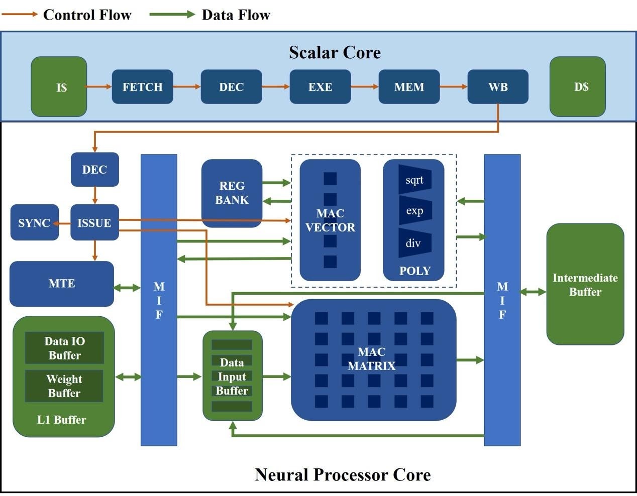
The figure below illustrates a high-level overview of the NeuralScale architecture. The key components include a RISC-V scalar core and a neural processor core. The scalar core fetches and decodes all instructions, and dispatches the instructions to the correct path based on their types. Scalar instructions are executed in order in the scalar pipeline while vector instructions flow through the scalar pipeline to the neural processor core.
The neural processor core combines the features of vector processors and AI inference accelerators. As shown in the figure below, the computation components include a MAC vector for executing vector operations, a MAC matrix for executing matrix operations, and a POLY module for complex arithmetics like exp, div, and sqrt computations. On-chips memory components include a vector register file (the REG Bank module) as well as three local buffers, named L1 Buffer, Data Input Buffer, and Intermediate Buffer respectively.
The neural processor core’s pipeline is divided into 4 stages in concept: decode, issue, execute, and write-back. Vector instructions are decoded into micro-ops in the decode unit and then dispatched to the issue unit. The issue unit issues instructions to corresponding execution units based on their operation types. There are three execution units, a vector MAC engine (VME), a matrix MAC engine (MME), and a memory transmission engine (MTE) for different operation types. The issue unit maintains three instruction buffers tracking the state of all inflight instructions in each execution unit. A dispatched instruction from the decode unit will be buffered according to its operation type and will be removed once it’s committed by the execution unit. All instructions will be issued in order, and an instruction can be issued only when there is no address overlap with inflight instructions. The issue unit can issue three instructions at most. All three execution units can work simultaneously in this case, and hence memory latency can be partially hidden by computation, which lifts overall performance. After execution, the results will be written back to vector registers or local buffers.
The RISC-V Vector extension (RVV) enables processor cores based on the RISC-V instruction set architecture to process data arrays, alongside traditional scalar operations to accelerate the computation of single instruction streams on large data sets. NeuralScale implements standard extensions including the base RVV extension (v0.8) and customized vector extensions with fixed-width 32-bit instruction format. We use the custom-3 opcode (11111011) in the RISC-V base opcode map as the major opcode for customized vector extensions, marked as OP-VE. All customized vector extensions keep the source (rs1 and rs2) and destination (rd) registers at the same position as the base RISC-V ISA does to simplify decoding, as shown in the table below.
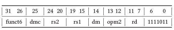
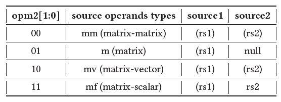
The opm2 field encodes the source operand types and source locations. For a vector or matrix operand, the general-purpose register provides the memory address of the values, marked as (rsx). The matrix operation directions are encoded using the dmc and dm fields. Taking matrix-vector additions for example, {𝑑𝑚𝑐, 𝑑𝑚} = 10 indicates adding a matrix with a row vector while {𝑑𝑚𝑐, 𝑑𝑚} = 01 indicates adding a matrix with a column vector. The funct6 field encodes operation types, including addition, subtraction, multiplication, accumulation, etc. Typical operations such as convolutions and activation functions in AI inference workloads are all covered.
A total of more than 50 customized instructions are extended in addition to the base RVV extension. For many matrix-related operations, information such as height and width of the matrix cannot be encoded within the 32-bit fixed-width instruction. Therefore, 22 unprivileged vector CSRs are added to the base RVV extension. Customized vector CSRs can only be updated with CSR instructions defined in the base scalar RISC-V ISA. The values should be properly set to match application needs.
STC P920: An Industrial SoC Implementation
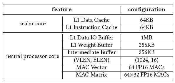
Based on the NeuralScale architecture, we implement an industrial SoC platform named P920 for AI inference in clouds. The scalar core adopted in P920 is the AndesCore N25F that is a 32-bit RISC-V CPU IP core with vector extension support. The scalar core has a separated L1 Data Cache and L1 Instruction Cache, each of 64KB. The neural processor core has a 1MB L1 Data IO Buffer, a 256KB L1 Weight Buffer and a 256KB Intermediate Buffer. The size of each local buffer in the neural processor core is selected based on experimental statistics of typical AI inference workloads, which helps to avoid frequently exchanging data between on-chip memory and external memory. The MAC vector in the neural processor core has 64 MAC units, and the MAC matrix in the neural processor core contains 64 × 32 MAC units. Each MAC unit supports both FP16 and INT8 arithmetics, which can be dynamically switched according to the operation type of each instruction.
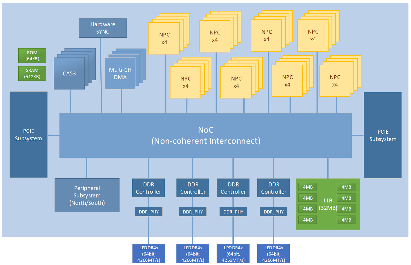
The figure below shows a high-level overview of the P920 architecture. The key components include 32 NeuralScale cores, a 32MB last level buffer (LLB), a hardware synchronization (HSYNC) subsystem, two PCIe subsystems, four DDR subsystems, a peripheral subsystem, and a CPU subsystem. All components are connected through an NoC with a regular 4×6 mesh-based topology. The links between each component and an NoC router, and the links between NoC routers are all bidirectional. The NoC separates control flow and data flow to lift data transmission efficiency. The control bus is 32 bits wide in each direction and the data bus is 512 bits wide in each direction. At 1.0 GHz, each direction provides up to 64𝐺𝐵/𝑠 bandwidth or 128𝐺𝐵/𝑠 combined. The 32MB LLB is split up into eight separated small LLBs of 4MB each. The small LLBs are connected to the NoC independently, providing 1𝑇𝐵/𝑠 memory bandwidth in total. Meanwhile, they are evenly distributed in the NoC so that other nodes can access an LLB within a small latency. As there are 32 NeuralScale cores in total, an HSYNC subsystem is used to manage how these cores cooperate and synchronize. NeuralScale cores can be divided into up to 16 groups by the HSYNC subsystems, and the number of cores in each group is configured by the application.
TensorTurbo: an E2E Inference Stack for STC P920 NPU
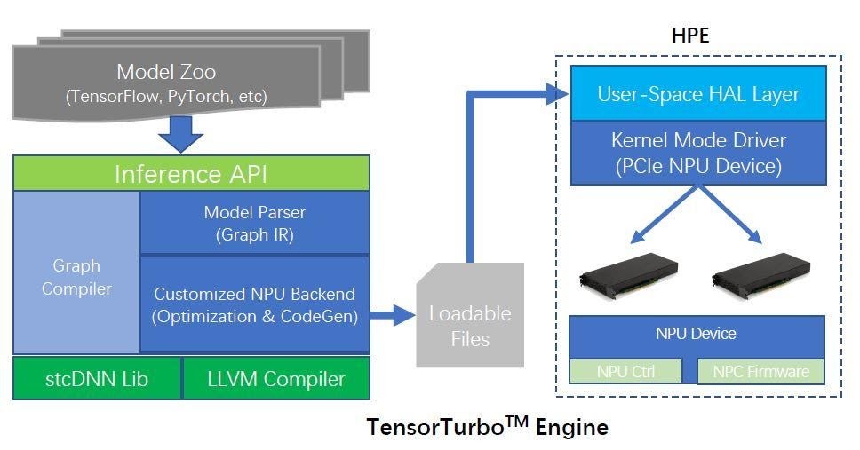
We implement an end-to-end inference stack named TensorTurbo for P920 that enables fast and efficient deployment of customers’ pre-trained AI models, as shown in Figure 4. TensorTurbo is mainly comprised of a graph compiler and a heterogenous program engine (HPE). The graph compiler is based on TVM and has been deeply customized for NeuralScale architecture. It provides C++ and python inference API for popular deep learning frameworks including TensorFlow, PyTorch, MxNet, and Keras. Graph intermediate representations (GIRs) from different frameworks are imported as unified TensorTurbo IRs via the inference API. The graph compiler then applies graph schedule, operators schedule, tiling strategies within an operator, among other optimizations to find the fastest implementation leveraging the hardware features at the most. The HPE provides high-level CUDA-style runtime APIs in the hardware abstraction layer (HAL), enabling functions like device management, kernel launch and management, memory management, etc. The HPE also provides utilities including GDB debug tool, performance profiling tool, and system monitor interface tool via accessing P920’s debugging features (event logging, performance counters, breakpoints).
Evaluation Results
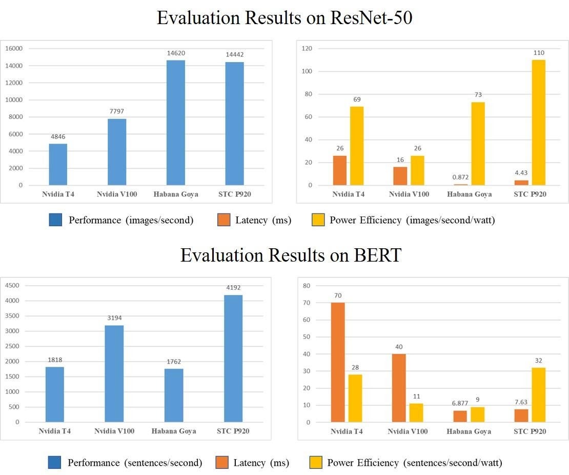
P920 was fabricated using TSMC’s 12nm FinFET technology and the total area is 400𝑚𝑚2 . It delivers 256 TOPS (INT8) and 128 TFLOPS (FP16) peak compute performance with a thermal design power of 130𝑊 under 1.0 GHz working frequency. We conduct a detailed performance evaluation of P920 with two typical AI inference workloads in clouds: the ResNet-50 CNN model for vision tasks and the BERT model for NLP tasks. As a comparison, experiments are also conducted on two GPU devices (Nvidia T4 and Nvidia V100) and an AI chip (Habana Goya).
The performance results include throughput, power efficiency, and latency of the four platforms are shown in the figure below. Compared to the GPUs, our P920 chip takes the lead in all the three aspects on both ResNet and BERT. Compared to the the Habana Goya chip, our P920 takes the lead in throughput and power efficiency. To be specifc, P920 delivers close throughput on ResNet and 2.37 times throughput on BERT. Besides, P920’s power efficiency is 1.50 times of the Habana Goya chip on ResNet and 3.56 times of the Habana Goya chip.
What’s Next?
NeuralScale takes advantage of customized RISC-V vector extensions to improve programmability and performance. Evaluations on our industrial product P920 demonstrate that our processor can achieve state-of-the-art inference performance on both CNN and NLP tasks. We’re about to mass produce the P920 chip to provide high-performance, high-efficient and high-programmability solutions for AI computing in clouds. Meanwhile, we plan to release ~30 optimized NN models for STC P920 chip to cover as much application needs as possible. Optimizations on NeuralScale will also be done in future work to further lift overall performance for our next-generation products.
“The simple, modular architecture and extensibility of the RISC-V ISA made the design of our NPC possible. This design freedom enabled us to create an extremely powerful computing core for neural networks that is also super power-efficient, scalable and programmable,” said Mark Zhan at Stream Computing. “We look forward to collaborating with the RISC-V community to drive more open source AI innovation for commercial applications.”