
Machine learning (ML) recommendation workloads have demanding performance and memory requirements and, to date, have largely been run on servers with x86 processors. To accelerate these workloads (and others), Esperanto Technologies has implemented over 1,000 low-power RISC-V processors on a single chip along with a distributed on-die memory system. The ET-SoC-1 chip is designed to compute at peak rates between 100 and 200 TOPS and to be able to run ML recommendation workloads while consuming less than 20 W of power. Preliminary data presented at the Hot Chips 33 Conference projected over a hundred times better performance per watt for an Esperanto-based accelerator card versus a standard server platform for the MLPerf Deep Learning Recommendation Model benchmark.
Watch the video from Stanford Online or read the paper originally published in IEEE Micro, vol. 42, no. 03, pp. 31-38, 2022 below.
Introduction
The ET-SoC-1 chip is implemented in TSMC 7-nm technology using over 24 billion transistors. The chip can operate standalone or as an accelerator and has three types of RISC-V-compatible processors designed by Esperanto. A single 64-bit RISC-V-compatible service processor helps with overall system boot. 1,088 64-bit ET-Minion RISC-V-compatible processors do most of the computing for ML applications. Four 64-bit ET-Maxion RISC-V-compatible processors are provided for high single-thread performance use, such as running an operating system. The chip has over 160 million bytes of on-die memory for local computation and LPDDR4x dynamic random-access memory (DRAM) controllers for accessing up to 32 GB of external memory. Eight lanes of PCIe Gen4 are provided for communication with a host processor.
This chip is designed to compute at peak rates between 100 and 200 TOPS, depending on the operating frequency of the ET-Minions. For many workloads, the chip operates using less than 20 W of power.
ML Recommendation Requirements
Machine learning (ML) recommendation workloads in hyperscale datacenters have some of the most demanding performance and memory requirements and, to date, have largely been run on servers with x86 processors. Often these servers have an available slot for a PCIe accelerator card, but an accelerator card needs to meet some key requirements.
- First, the performance of the accelerator card needs to substantially exceed the performance of the x86 host central processing unit (CPU), which means the card needs to reach computation rates of 100–1,000 TOPS.
- Second, the accelerator card must fit into existing infrastructure, where there may only be one PCIe slot available per server, and that slot will have a limited power budget, typically 75–120 W. Google published a paper on 10 key lessons from their TPU design experience; one of those lessons is that for inference deployment at global scale, solutions must be air-cooled,1 so low power is very important.
- While a lot of inference can be done with eight-bit integer data, potential customers also required hardware support for both 16- and 32-bit floating point.1,2
- An accelerator card should have at least 100 GB of storage to avoid excessive movement of data from the host.3
- Having at least 100 MB of on-die memory can significantly improve performance and substantially reduce many off-die memory references, which in turn can increase performance and reduce power.5
- Recommendation problems have both dense compute and very large sparse memory accesses. In this way, they are quite different from the purely dense compute CNN operations one might see in the ResNet50 benchmark. Computation mixed with very large, sparsely accessed data is challenging because the latencies to off-chip memory are very large, which may cause processing to stall.
- Finally, because ML workloads are rapidly evolving, fixed function hardware can quickly become obsolete, so the use of more general-purpose programmable solutions is highly recommended.4 Esperanto picked the RISC-V instruction set as the foundation for its general-purpose programmable solution.
Esperanto Takes a Different Approach
Esperanto’s approach is different from most other inference accelerators in several ways.
Some other solutions use one giant hot chip that uses up the entire power budget of the accelerator card. Esperanto’s approach is to use multiple low-power chips that still fit within the power budget.
Some use expensive, high-power on-package HBM DRAM to get more memory bandwidth. Esperanto’s approach distributes the processing and input/output (I/O) across multiple chips, so performance, memory capacity, and memory bandwidth scale as more chips are added, making lower cost LPDDR4X DRAM a practical solution.
Use of large array multipliers is common in other AI chips, and they do work well for dense computations like CNNs and can generate great ResNet50 scores. But overoptimizing for CNNs compromises flexibility, and often these solutions do not perform well on sparse memory accesses to off-chip memory.
Esperanto began with general-purpose RISC-V cores instead, adding custom vector and tensor instructions to boost computational throughput. This results in a far more flexible solution. Further accelerating sparse accesses to large memory, the Esperanto solution supports thousands of threads to help hide long-memory latencies.
Single-chip solutions often push for the highest operating voltages and frequencies, but this comes at the expense of poor energy efficiency and high operating power.
For chips depending on specialized hardware (e.g., array multipliers) and only a few (10–20) CPU cores, any problem that does not exactly map onto the specialized hardware must fall back to the limited number of CPU cores. In the Esperanto solution, the full parallelism of thousands of general-purpose cores is always available to speed up execution.
Single-chip solutions often push for the highest operating voltages and frequencies, but this comes at the expense of poor energy efficiency and high operating power. Esperanto realized that transistors, particularly 7-nm FinFET’s, are much more energy efficient when operated at low voltages. Low-voltage operation also significantly reduces operating power. To take advantage of this low-voltage energy efficiency required Esperanto to make substantial innovations to both circuits and modifications to the architecture of the RISC-V cores.
Low-Voltage Operation
Esperanto performed an experiment that demonstrates the value of low-voltage operation in achieving the best recommendation performance for our 120-W card using a maximum of six chips.
Figure 1 shows a graph of the energy efficiency of a thousand ET-Minion cores running our internal recommendation benchmark at different operating voltages. In this experiment, we model the cores as being resynthesized for each particular voltage point, as a core optimized for a high voltage and high frequency will have more capacitance from bigger buffers to overcome wire delay than a core optimized for lower operating voltages. For simplicity of this example, we assume that the only power we have to worry about is the ET-SoC-1 chip.
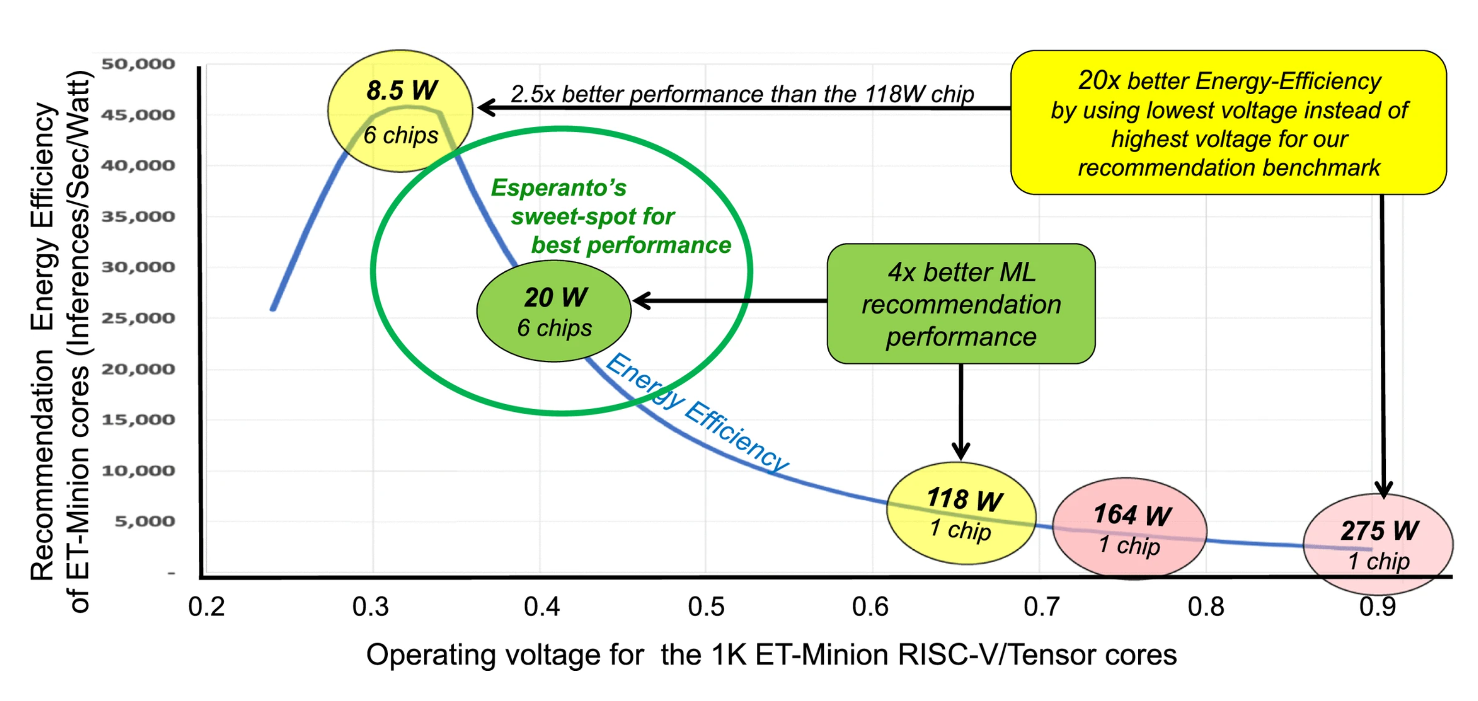
Figure 1. Inferences/second/watt (energy efficiency) versus operating voltage and number of chips.
A common approach would be to try to run at the highest voltage to get the highest frequency, but if we did this, just one of our chips might use 275 W, way over the 120-W limit, so this does not work.
Reducing the operating voltage to 0.75 V, the nominal voltage in 7 nm, would result in 164 W, still way too high.
Just to get under 120 W on a single chip, we would have to reduce the voltage down to about 0.67 V, but then that one chip would use up the entire power budget.
If we operate at the best energy-efficiency point (0.3 V), each chip will consume only 8.5 W, and six chips will fit in the 120-W budget with room to spare.
With six chips the performance would be 2.5 times better than the 118-W single-chip solution, and the energy efficiency is 20 times better than trying to operate at the highest voltage.
To maximize performance however, we should use up the entire power budget, and if we operate around 0.4 V, one chip would take about 20 W, meaning we could use six chips and be within the 120-W power budget.
By using the entire available power budget, we end up with four times better recommendation performance than that of a one-chip solution.
Esperanto’s sweet spot for achieving best performance will usually be for operating our ET-Minions between 300 and 500 mV, that is, nearest the best energy efficiency points.
Low-voltage operation is a key differentiator for Esperanto’s ET-Minion design.
Putting the Cores Together, Starting With the ET-Minions
The ET-Minion is Esperanto’s proprietary custom-built processor compatible with the 64-bit RISC-V integer instruction set. The RISC-V integer pipeline is shown in yellow in the block diagram in Figure 2, which is drawn roughly to scale with the area of each unit. Esperanto has added its own vector/tensor unit optimized for common ML data types, and you can see that the vector/tensor unit takes far more area than the integer pipeline, supporting our premise that area overhead for RISC-V is small.
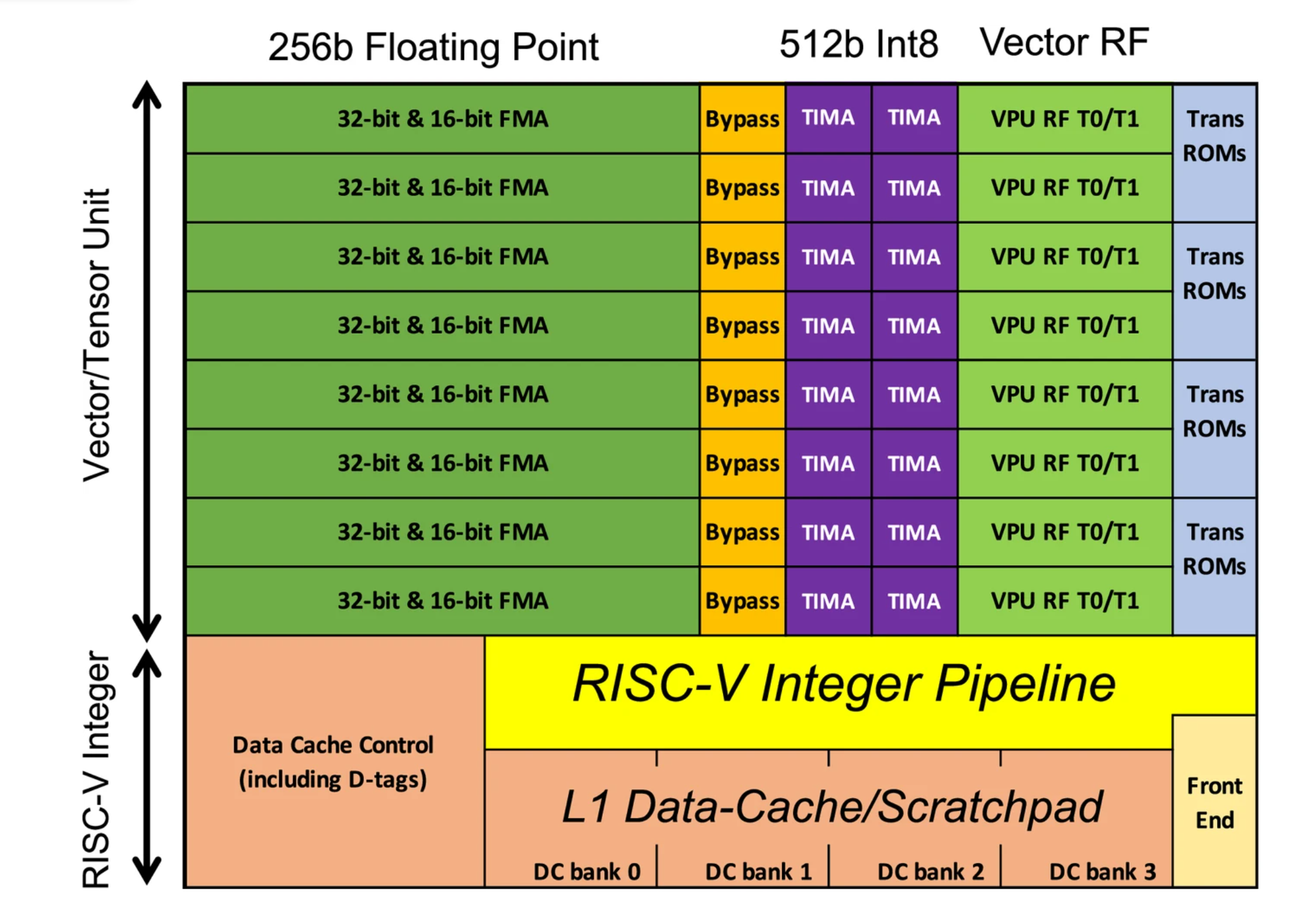
Figure 2. ET-Minion RISC-V core with vector/tensor unit and L1 cache/scratchpad memory, optimized as a unit for low-voltage operation to improve energy efficiency.
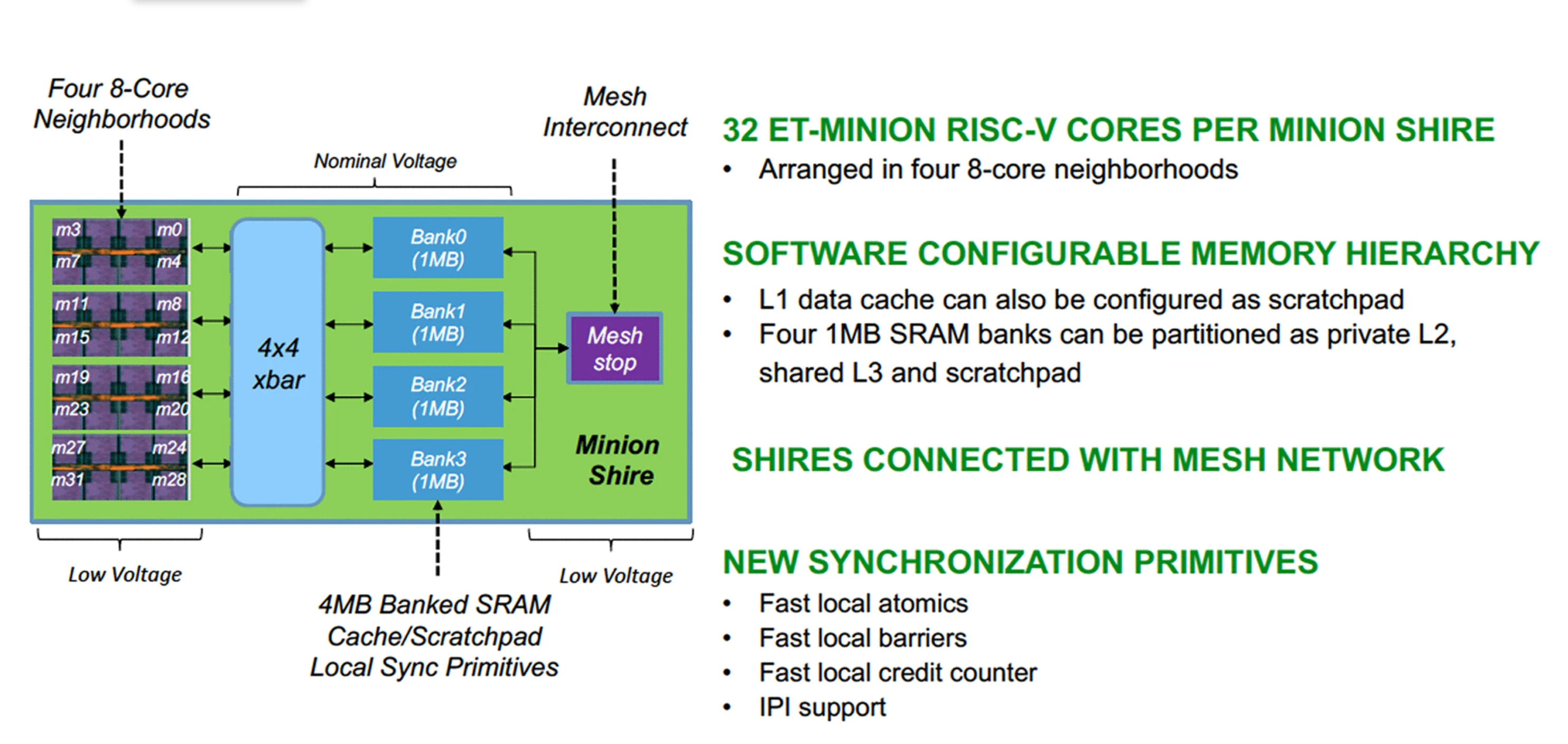
Figure 3. Thirty-two ET-Minion cores and 4 MB of memory form a Minion shire.
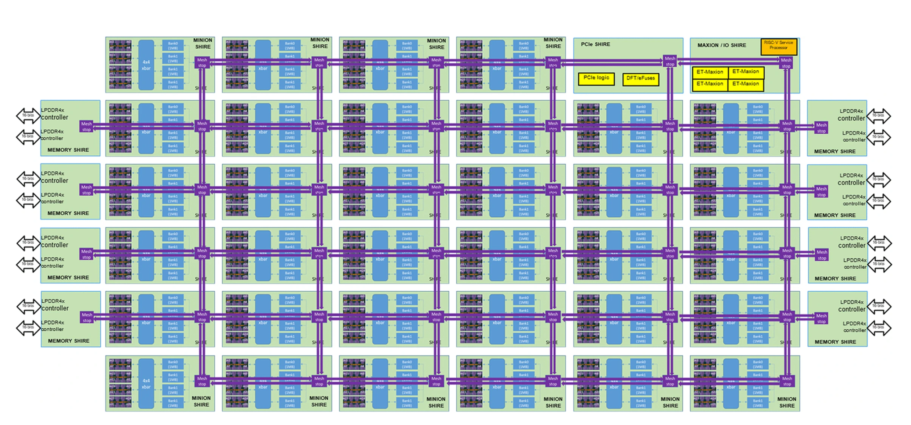
Figure 4. Internal block diagram of the ET-SoC-1 chip.
The core uses an in-order pipeline optimized to have very few gates per pipeline stage to improve megahertz when operated at low voltages. For timing and other CAD tools, we had libraries recharacterized at 0.4 V. Two hardware threads of execution are supported. To simplify physical design, the entire ET-Minion, including its 4-KB L1 caches, operates on a single low-voltage power plane.
The vector/tensor unit is optimized for 8-bit integer, 16-bit floating point, and 32-bit floating-point operations, which are the most common ML data types used for inference. Integer operations were deemed the most important, so the integer vector width is 512 bits (64 bytes). Integer multiply–add operations perform 128 8-bit operations per cycle, with the results accumulating to 32-bit integers. The floating-point vector width is 256 bits, resulting in 16 32-bit single-precision operations or 32 half-precision operations per cycle.
As a large percentage of execution time is spent performing tensor operations, Esperanto added new tensor instructions that utilize the full vector width every cycle and run for up to 512 cycles. A single-tensor instruction can perform up to 32,000 operations, greatly reducing instruction fetch bandwidth requirements.
Tensor instructions manage data movement as well as compute and can utilize the data cache as a scratchpad. Instead of a loop of instructions to compute a tensor, use of a single-tensor instruction reduces instruction fetch bandwidth requirements, which in turn further reduces power consumption. During these long tensor instructions, the RISC-V integer pipeline is put to sleep, further making the overhead for providing RISC-V compatibility almost negligible.
Physical design plays an important role in chip architecture as 7-nm wires are relatively slow. We found it convenient to group eight ET-Minion cores together before wire length became a problem. These groups of eight ET-Minion cores are called a neighborhood, and we were able to use their physical proximity to make several architectural improvements. We were able to save power and improve performance by allowing neighborhood cores to closely cooperate. For example, eight ET-Minion cores share a single large instruction cache; this was far more efficient than having each core having its own instruction cache with redundant copies of the same code.
As another example, when one ET-Minion is doing a load from L2 cache, it is likely that the other seven minions in the same neighborhood will also fetch the same data. Rather than doing eight separate loads from the L2 cache of the same data, the ET-Minions have a “cooperative load” feature that allows all eight cores to receive the data using only one transfer from the L2 cache. These are just a few of Esperanto’s innovations that allow highly parallel programs to compute more effectively than an array of standard processors.
32 ET-Minion CPUs and 4-MB Memory Form a “Minion Shire”
Four of these 8-core neighborhoods are put together along with 4 MB of memory to form a 32-core “Minion Shire.” The memory is implemented as four 1 MB SRAM banks connected to the neighborhoods through a 512-bit crossbar switch. These SRAM banks operate near the process-nominal supply voltage to allow higher density than the smaller caches within each core. Each bank can be partitioned by software to provide a mix of scratchpad memory, L2 cache private to the Shire, or L3 cache globally accessible across the entire chip via a global shared address space.
Shires are connected to each other via an on-chip mesh interconnect operated on its own low-voltage domain. To enhance the performance of these cooperating parallel processes, Esperanto has added several new synchronization primitives.
Putting It All Together on a Single Chip
Now we can see how the entire chip fits together in this block diagram that also roughly corresponds to the physical layout on the chip. A total of 34 ET-Minion shires contain 1,088 ET-Minion processors. On the left- and right-hand sides, eight-memory shires contain the LPDDR4x DRAM controllers. One Maxion/IO shire contains the four ET-Maxions and most of the other small I/O signals as well as a hardware root of trust.7 One PCIe shire contains a Gen4 PCIe interface that can be configured as one eight-lane interface or two independent four-lane interfaces. Maximum chip power can be set with a software API, but for recommendation tasks, we expect a typical operating point will be under 20 W.
Using the ET-SoC-1 CHIPS IN A REAL SYSTEM
Esperanto’s low-power technology allows six Esperanto chips and 24 64-bit-wide DRAM chips to fit into the 120-W power budget of the customer’s PCIe card slot. One accelerator card can hold up to 192 GB of DRAM providing up to 819 GB/s of memory bandwidth. By using multiple chips, we can effectively have a 1,536-bit-wide memory interface using low-cost and low-power LPDDR4x DRAM, which would have required too many pins for a single-chip solution. This one accelerator card has 6,144 cores and 12,288 threads of execution to hide memory latency for the memory intensive portions of recommendation models.
For this application, each Esperanto chip is mounted on an Open Compute Project Dual M.2 module that also contains DRAM, flash memory, and power supply circuitry. Six of these modules will fit on an OCP Glacier Point version 2 card. Peak performance for this one card would be 836 TOPS (INT8) when all ET-Minions operate at 1 GHz.
Figure 5 shows an example of how Esperanto’s chip could be deployed at scale in existing OCP data centers.8 Two Glacier Point v2 cards fit into a Yosemite v2 server sled for 12 ET-SoC-1 chips per sled. Four Yosemite sleds fit into a rackmount OCP “cubby” and eight cubbies fit into an OCP rack, so each rack holds 384 chips.
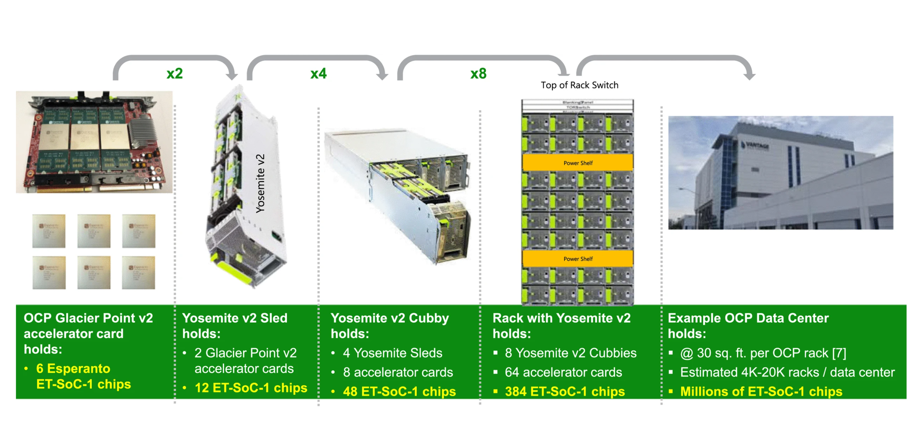
Figure 5. Example of how the ET-SoC-1 could be deployed at scale in OCP data centers.
With thousands of racks in a large data center, a large data center could potentially deploy millions of accelerator chips.
ML Recommendation Performance
We will now compare performance on the MLPerf Deep Learning Recommendation Model benchmark using scores reported on the MLCommons.org website by the respective vendors and Esperanto’s projected performance.9
Figure 6 shows the performance comparison. The light green bars compare the relative performance of each accelerator card to the performance contributed by one Intel Xeon server processor. The dark green bars compare the relative performance per watt of each accelerator card to the TDP power of one Xeon. So, for example, the MLPerf DLRM score for Intel was reported as 24,630 using eight Xeons. Assuming linear scalability and dividing by eight, we get 3,079 samples per second for one Xeon. The performance and power numbers used for comparison in the bar charts are shown here in bold.
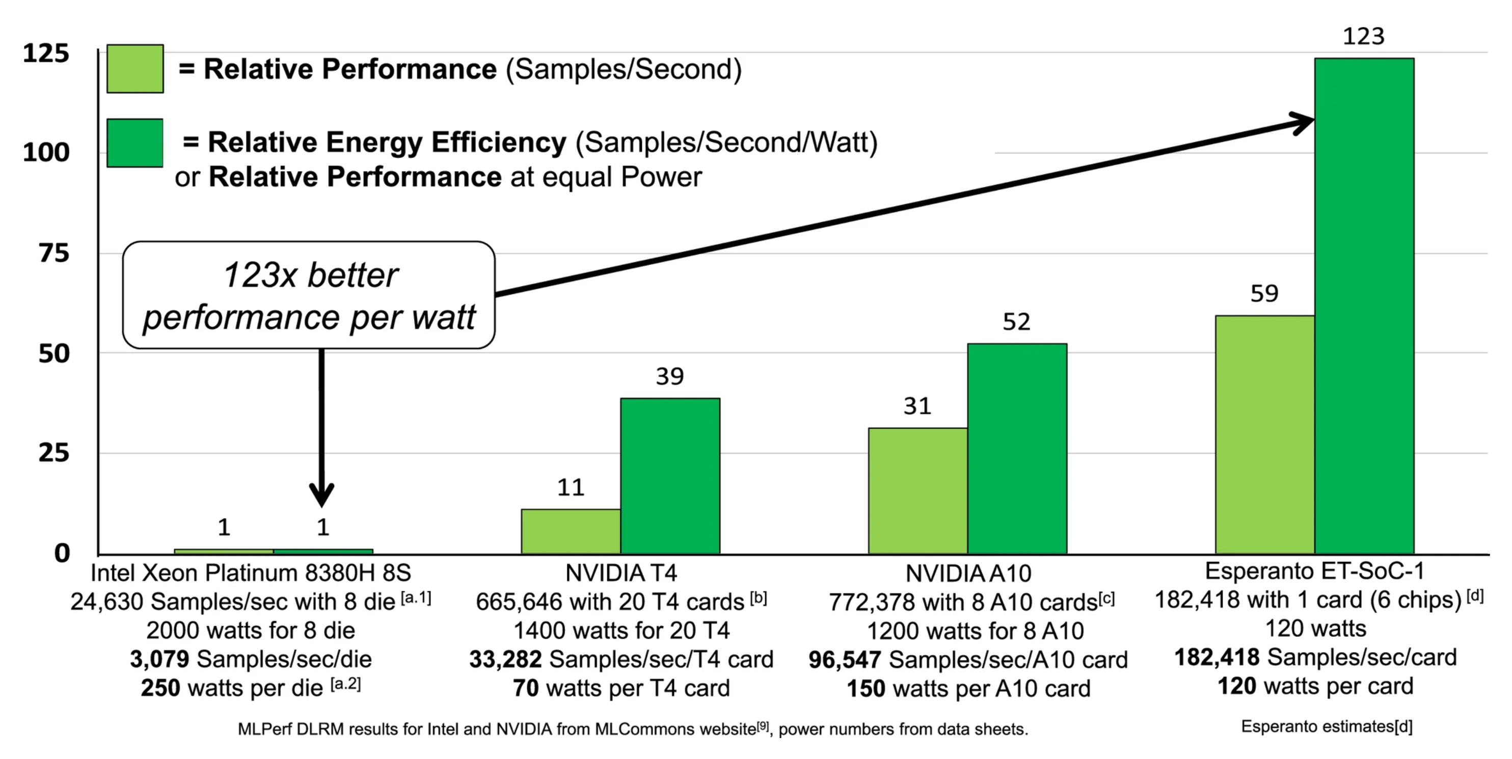
Figure 6. MLPerf DLRM results for Intel and NVIDIA from MLCommons website,9 power numbers from datasheets, and Esperanto projections (see “Additional Source Information”).
The Esperanto ET-SoC-1 is the highest performance commercial RISC-V chip announced so far.
One 120-W accelerator card with six Esperanto chips delivers 59 times the performance and 123 times the energy efficiency of one 250-W Xeon. We suggest that performance per watt is actually a better metric of performance, since everyone ought to be measured at similar power usage. Esperanto expects our performance per watt to be over 123 times better than the server chip.
Summary Statistics and Chip Status
The Esperanto supercomputer on a chip has been fabricated in TSMC 7-nm technology and contains over 24 billion transistors.
It has a die area of 570 mm2 and uses 89 mask layers.
All the Esperanto performance numbers presented at Hot Chips were projections based on gate-level simulations of the entire chip on a large Synopsys Zebu hardware emulation system.
Figure 7 shows a die plot and the 7-nm silicon mounted in a package. Esperanto received ET-SoC-1 silicon in our labs in August 2021, just prior to the Hot Chips conference and since that time the chip has been successfully operated.
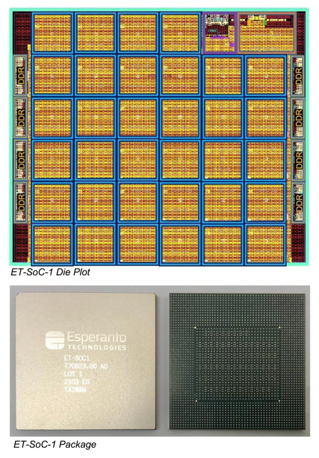
Figure 7. ET-SoC-1 die plot and package.
Summary
The Esperanto ET-SoC-1 is the highest performance commercial RISC-V chip announced so far.
- It has the most 64-bit RISC-V cores on a single chip.
- It has the most RISC-V aggregate instructions per second on a single chip.
- It has the highest number of TOPS on a chip driven by RISC-V cores.
- Esperanto’s low-voltage technology provides differentiated RISC-V processors with the best performance per watt.
Energy efficiency matters, and we suggest that the best way to compare performance is to compare performance per watt. Making an efficient parallel-processing system required many innovations and tradeoffs between the processor and memory system architecture, and the circuits and low-voltage techniques that improve energy efficiency and avoid dark silicon.10 Now that this architecture is done and proven in silicon, we can take this modular architecture and easily scale it up or down and port it to other semiconductor processes.
Additional Source Information
- Submitter: Intel; MLPerf DLRM score 24,630: Inference Data Center v0.7 ID 0.7-126; Hardware used (1-node-8S-CPX-PyTorch-BF16); BF16; [Online]. Available: https://mlcommons.org/en/inference-datacenter-07/.
- Intel 8380H Processor TDP power of 250 W. [Online]. Available: https://ark.intel.com/content/www/us/en/ark/products/204087/intel-xeon-platinum-8380h-processor-38-5m-cache-2-90-ghz.html.
- Submitter: NVIDIA; T4 MLPerf DLRM score 665,646: Inference Data Center v0.7 ID 0.7-115; Hardware used (Supermicro 6049GP-TRT-OTO-29 (20x T4, TensorRT)); INT8. [Online]. Available: https://mlcommons.org/en/inference-datacenter-07/.
- Submitter: NVIDIA; A10 MLPerf DLRM score 772,378: Inference Data Center v1.0 ID 1.0-54; Hardware used (Supermicro 4029GP-TRT-OTO-28 (8x A10, TensorRT)); INT8. [Online]. Available: https://mlcommons.org/en/inference-datacenter-10/.
- Internal estimates by Esperanto for MLPerf DLRM: Inference Data Center v0.7; ET-SOC-1; Unverified result is from Emulated/Simulated presilicon projections; INT8; Result not verified by MLCommons Association.
References
- N. Jouppi , “Ten lessons from three generations shaped Google’s TPUv4i,” in Proc. ACM/IEEE 48th Annu. Int. Symp. Comput. Archit., 2021, pp. 1–14.
- J. Park , “Deep learning inference in Facebook data centers: Characterization, performance optimizations and hardware implications,” 2018, arXiv:1811.09886v2.
- M. Anderson , “First generation inference accelerator deployment at Facebook,” 2021, arXiv:2107.04140v1.
- M. Smelyanskiy, “Challenges and opportunities of architecting AI systems at datacenter scale,” in Proc. Linley Fall Processor Conf., 2019.
- M. Smelyanskiy, “AI system co-design: How to balance performance & flexibility,” in Proc. AI Hardware Summit, 2019.
- P. Xekalakis and C. Celio, “The Esperanto ET-Maxion High Performance Out-of-Order RISC-V Processor,” in Proc. RISC-V Summit Presentation, 2018. [Online]. Available: https://www.youtube.com/watch?v=NjEslX-t0Q
- “Esperanto Maxes out RISC-V – High-End Maxion CPU Raises RISC-V Performance Bar,” Microprocessor Rep., pp. 1–5, Dec. 10, 2018.
- “The Case for the Infinite Data Center,” Gartner, Data Center Frontier, 2012.
- MLPerf DLRM Inference Data Center v0.7 and v1.0, 2021. [Online]. Available: https://mlcommons.org/en/
- M. B. Taylor, “Is dark silicon useful? Harnessing the four horsemen of the coming dark silicon apocalypse,” in Proc. 49th Ann. Design Autom. Conf., 2012.