

Recent rapid development of various applications represented by Deep Learning (DL) calls for a much-needed increase in established chip matrix computing capability. Therefore, CPU manufacturers strive to better support matrix instruction extension with the latest products like the Advanced Matrix Extensions (AMX) from Intel[1], the Scalable Matrix Extension (SME) from Arm[2], and the Matrix-Multiply Assist (MMA) from Power[3]. This blog summarizes and explores two different architecture choices of the matrix extension in a CPU.
Matrix multiplication Overview
The matrix extension in a CPU is mainly used to provide matrix multiplication instructions. The basic matrix multiplication operation is shown in Figure 1: each row of matrix A (M x K) times each column of matrix B (K x N), yielding one element of the resulting matrix C (M x N).
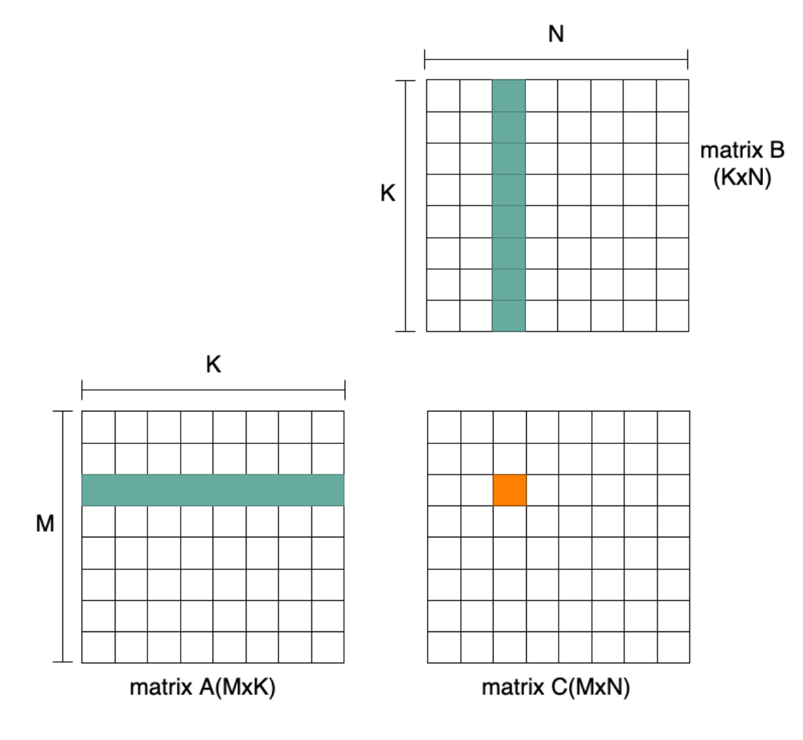
Figure 1 Matrix Multiplication Operation
The implementation of matrix multiplication is three nested loops shown as follows:
for (int row =0; row<M; row++) {

for (int col=0; col<N; col++) {

   for (int k=0; k<K; k++) {

          C[row, col] += A[row, k] * B[k, col]

}}}
In general, modern CPUs like Intel AVX, Arm NEON/SVE and the RISC-V Vector extension (RVV) exhibit good vector processing capability. Using vector instructions enables calculation of more than one result at a time. Figure 2 shows an example with the vectorization dimension of N.
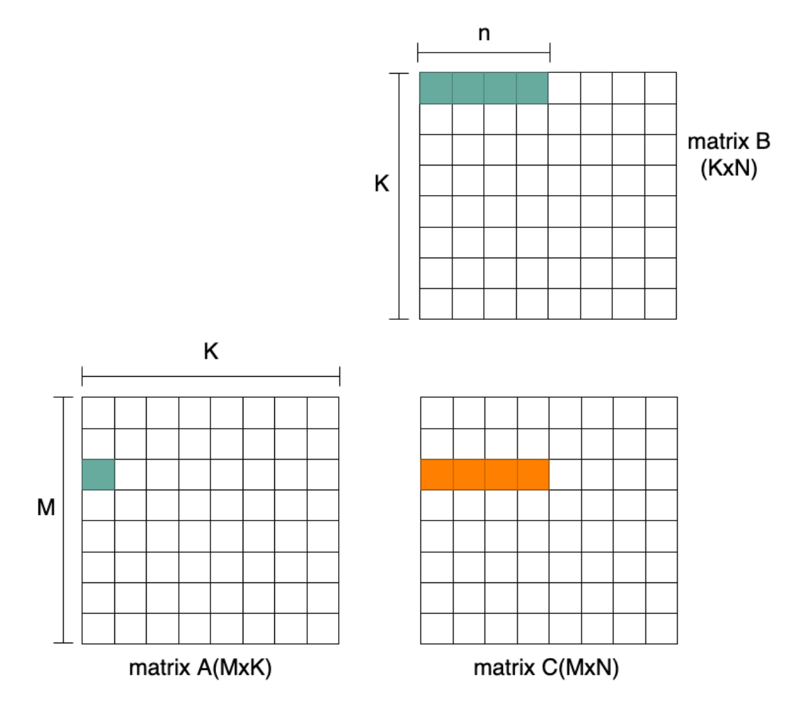
Figure 2: Vectorization Dimension of N
The measuring metric for matrix multiplication performance is Giga floating-point operations per second (GFLOPs) or Giga operations per seconds (Gops). Thus, the performance with vector instructions is determined by the vector length and the data width. Wider vectors have evolved over time bringing larger load/store bandwidth requirements. One way to further improve performance and efficiency is by supporting matrix multiplication instructions, which compute Cmn+= Amk* Bkn. The peak performance is reached when m*k*n multiply and accumulate operations are completed in each cycle, i.e. m*k*n*2 operations per cycle. Figure 3 illustrates a 2x2x2 multiplication instruction of 16 operations per cycle peak performance. With the same elements loaded the peak performance in Figure 3 is twice that of Figure 2.
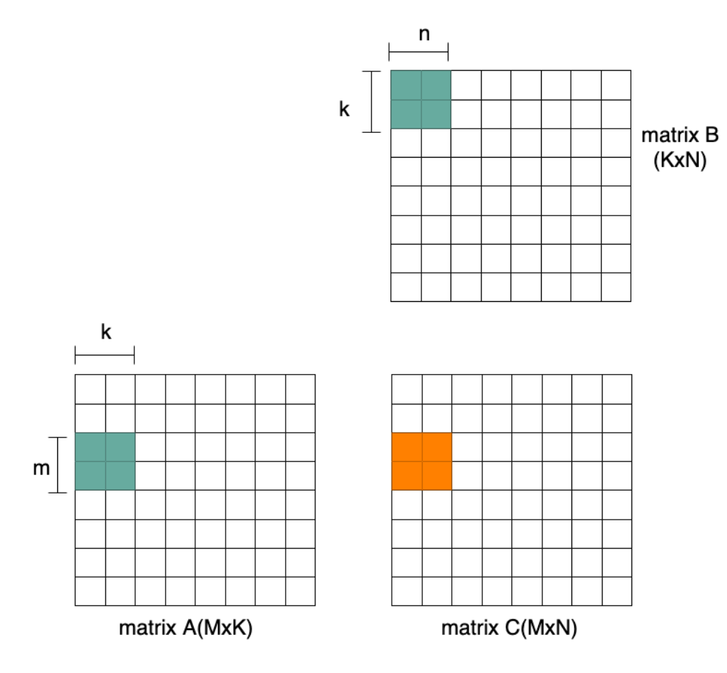
Figure 3 Matrix Multiplication Instruction Example
The goal of the matrix multiplication instruction design is to get higher performance with lower resource cost. Key hardware resource costs include matrix registers and matrix function units. In order to achieve the same performance, we will require the same resource cost for the function units. Therefore, the main trade-off is the matrix register file cost of different architectures, as it depends on matrix register size and register number.
The matrix register size is determined by the matrix size and data width. As the matrix operand is stored in the register, we make the assumption that A and B are the same size, i.e. m=n. Let’s assume the following: matrix A is m x k, matrix B is k x m and matrix C is m x m. The data width varies by applications. For example, in AI inference, a typical data width of a source operand is 8-bit, while an accumulator is 32-bit. Thus, matrix register size for matrix A and B is m*k*8 bits and m*m*32 bits for matrix C.
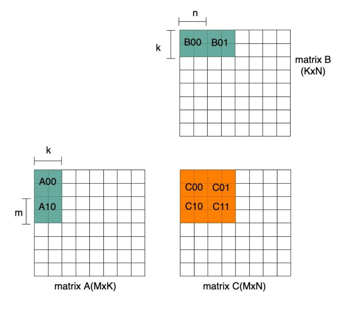
Figure 4 Matrix Register Assignment
Matrix multiplication algorithms tend to reduce the quantity of load/store memory access by: 1) reusing source operand by storing it in registers as much as possible and 2) accumulating results in registers as long as possible. As a consequence, the demand for more registers will increase. Assume the number of matrix registers required is 8, which are used to store two rows of A sub-block(A00/A10), two columns of B sub-block (B00/B01) and 4 intermediate C results. As shown in Figure 4, each matrix A is re-used twice as we multiply it by two matrix B.
We will summarize and explore two different architecture choices for matrix extension in CPUs and compare their resource cost of the same performance in the next section.
Architectures for matrix extension
The matrix extension can reuse existing vector registers to provide operands for matrix function units by treating vectors as two-dimensional matrices, i.e. architecture 1) due to the size difference, requirements on the width of destination operands are not guaranteed to be the same as that of the source. A particular accumulator register needs to be provided. As Figure 5 illustrated below, the source operands are stored in the vector register file. After matrix multiplication is completed, results are temporarily stored in the accumulator registers until the accumulation is done.
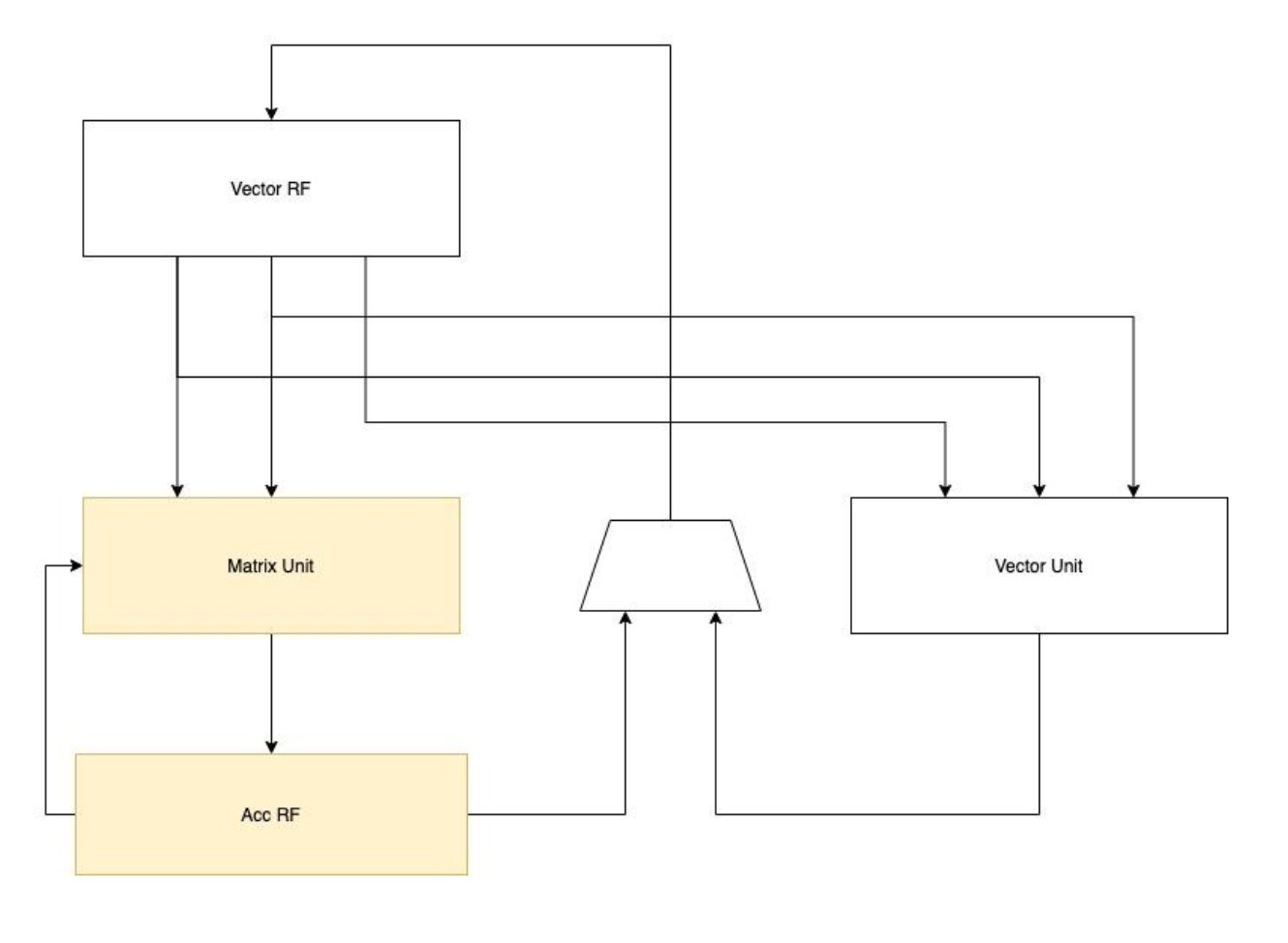
Figure 5 Architecture 1-Extending Accumulator Registers
In some special cases, it is not necessary to extend the accumulator registers: the destination and source operands share the same data width, or the destination is 2x width of source operands. For these scenarios, architecture 1 fits to be the best choice that minimum or zero resource cost will be incurred while vector registers being fully reused. Below in the table, various vector lengths are demonstrated in the matrix size without the requirement of accumulator expansion.
Table 1 Architecture 1 Example Design without Accumulator Registers
| M | K | N | Vector Length(bits) | Acc Length(bits) | Max Ops/cycle |
| 2 | 8 | 2 | 128 | 128 | 64 |
| 4 | 8 | 4 | 256 | 512 | 256 |
| 4 | 16 | 4 | 512 | 512 | 512 |
| 8 | 16 | 8 | 1024 | 2048 | 2048 |
Nonetheless, accumulator registers are still essential for alternating vector length or peak performance. The following discussion will base on the architecture with accumulator registers. A feasible proposal is to fix one dimension of the matrix and change others customized to different vector lengths, such as fixed K=4. The length of the accumulator register and peak performance of different vector register lengths are presented in the table below.
Table 2 Architecture 1 Example Design with Accumulator Registers
| M | K | N | Vector Length(bits) | Acc Length(bits) | Max Ops/cycle |
| 4 | 4 | 4 | 128 | 512 | 128 |
| 8 | 4 | 8 | 256 | 2048 | 512 |
| 16 | 4 | 16 | 512 | 8192 | 2048 |
| 32 | 4 | 32 | 1024 | 32768 | 8192 |
Another alternative is to extend two-dimension matrix registers without reusing vector registers. Matrix registers provide operands to matrix function units including accumulators as Figure 6 shows. Architecture 2 is more independent and flexible, which is more friendly to hardware design and software programming. Matrix extension can be completely decoupled from the vector unit and the vector unit does not get affected by changes of matrix unit. Higher matrix performance can be obtained for a given vector length.
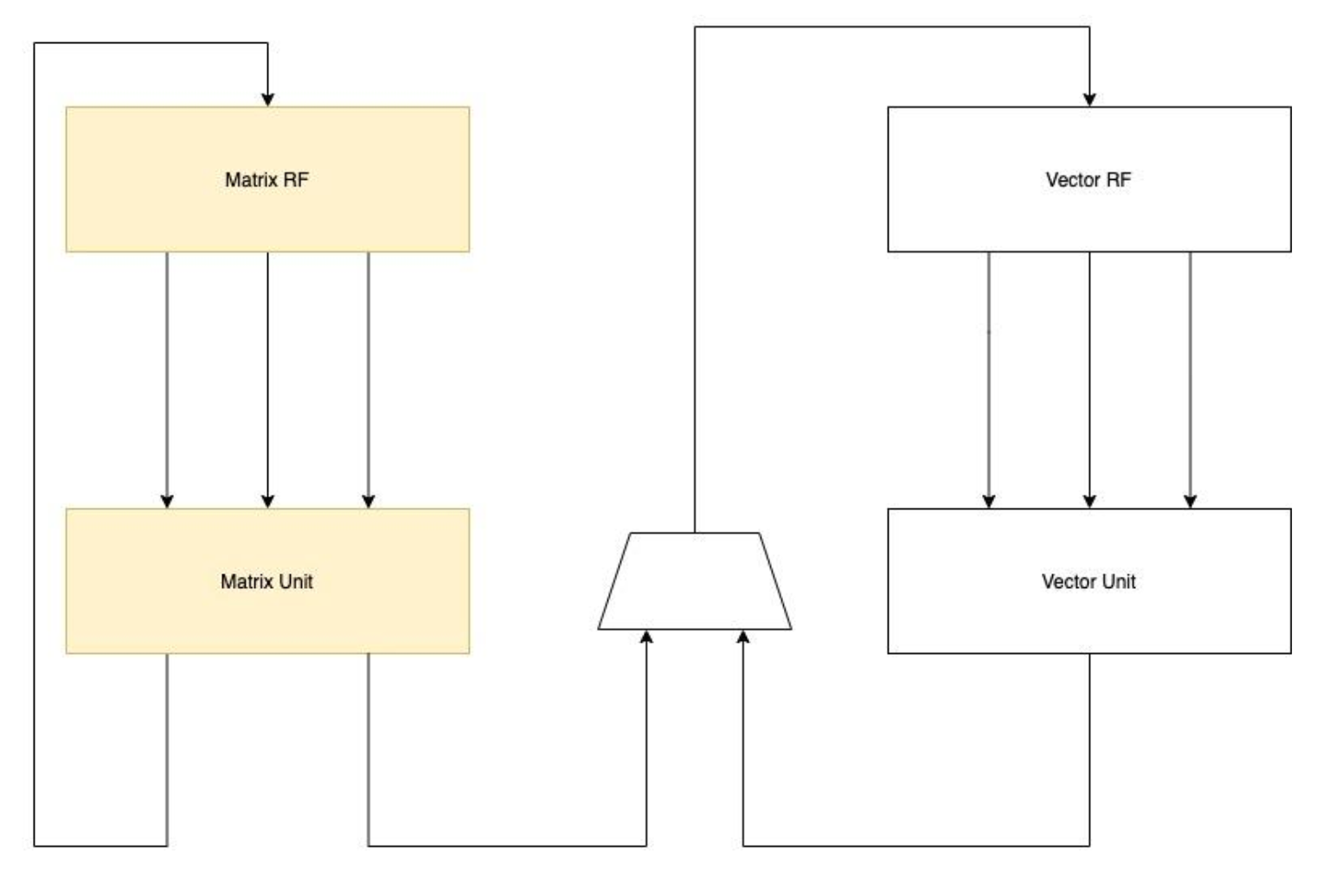
Figure 6 Architecture 2-Extending Matrix Register File
Considering the source and the destination operand width in bit are the same, the alternative design scheme of architecture 2 is as follows as the matrix register length increases:
Table 3 Architecture 2 Example Design
| M | K | N | Matrix Length(bits) | Max Ops/cycle |
| 2 | 8 | 2 | 128 | 64 |
| 4 | 16 | 4 | 512 | 512 |
| 8 | 32 | 8 | 2048 | 4096 |
| 16 | 64 | 16 | 8192 | 32768 |
The cost for the flexibility of architecture 2 may be the potential more resource overhead. Let us take a comparison of register resource overhead between the two architectures. If the vector length matches the matrix performance requirements, architecture 1 is obviously more resource efficient, i.e. 128 bits vector length for vector unit and 128 operations per cycle matrix unit of the example design in Table 2. However, with the increase of matrix performance requirements, architecture 1 needs to synchronously increase the vector length, i.e. 256 bits vector length for 512 operations per cycle matrix unit. Considering the additional vector register overhead brought by matrix extension, the resource overhead of architecture 2 is not necessarily larger than architecture 1. Moreover, as the width of the vector register increases, the resources of the vector unit may also increase accordingly or the scheme should be designed to support different vector lengths of vector and matrix units.
Summary
In this blog, two different architectures for matrix extensions in a CPU are presented and summarized: 1) The existing vector registers are treated as two-dimensional matrices to provide matrix operands and extending accumulator registers if necessary, and 2) Matrix registers are provided to decouple vector units and enable matrix function units to be more independent.
The advantage of architecture 1 is that it partially saves resources while reducing processor state. When the width of the vector register is fixed, some designs even needn’t add additional processor state. Architecture 2 has a larger computing scale, higher peak computing force and more flexible implementation. When the performance requirement changes, the program model and vector unit may be not affected. Both the two architectures have their disadvantages. The former needs to handle the performance limitation from the vector register length and the significant increase in accumulation register width for higher performance requirements. The latter should overcome the shortcoming of higher resource cost for lower peak computing force. T-Head XuanTie CPUs are extending matrix instructions to better support matrix operations. We aim for more targeted architecture selection to fit into various business scenarios with lower resource cost and more flexible implementation.
- Intel®Architecture Instruction Set Extensions and Future Features Programming Reference
- Arm® Architecture Reference Manual Supplement, The Scalable Matrix Extension (SME), for Armv9-A
- A matrix math facility for Power ISA™ processors