

Yuehai Chen, Huarun Chen, Shaozhen Chen
Guangdong University of Technology
In the China Postgraduate IC Innovation Competition this August, T-Head sponsored the design challenge: Building the Dual-core TEE security solution based on Xuantie Open E902. In this competition, there are lots of excellent designs, and some of the teams take the initiative to share their designs. The team “ReShaker” from Guangdong University of Technology won the first prize in the competition, they introduce their design in this blog.
Trusted Execution Environment (TEE) is an efficient way to secure information. To obtain higher efficiency, the building of a dual-core System-on-chip (SoC) with TEE security capabilities is the hottest topic. However, TEE SoCs currently commonly use complex processor cores such as Rocket, resulting in high resource usage; More importantly, the cryptographic unit lacks flexibility and ignores secure communication between the cores.
To address the above problems, we designed a dual-core TEE SoC based on RISC-V. First, a multi-level bus architecture with complete isolation of the TEE environment is built, and a Secure Core which supports acceleration of SHA1, AES and RSA algorithms integrated, RSA can be flexibly configured to five different key lengths; Furthermore, a secure boot process is Incorporated that is based on the Chain-of-Trust (CoT) to verify the authenticity and integrity of the loaded program. IOPMP is also designed to configure the access rights of the Rich Execution Environment (REE) CPU and the Secure Core. Finally, mailbox is employed for inter-core communication, and hierarchical access policy is proposed for data exchange to ensure the security of communication.
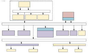
Figure 1. TEE SoC implementation using E902.
Multi-level Bus Architecture of TEE SoC
The architecture of SoC in this work is shown in Figure 1. The proposed architecture uses two E902 CPUs developed by T-Head as processor cores. And the CPU running in the TEE environment is called the TEE CPU, and the CPU running in REE environment is called REE CPU. As shown in Figure 1, the dual-core SoC uses a hierarchical bus design with three layers. The first layer of the bus located in the Isolated System is under a secure world called FL-AHB. As the master device, the TEE CPU can access all the devices under this bus, such as BootRom. This layer of the bus does not provide access to devices other than the master device. Therefore, the Isolated System is a completely isolated environment, and internal data cannot be accessed directly. The second-layer bus is the bus for building the TEE system (SL-AHB), and the TEE CPU can access all the slave devices on this bus layer. Meanwhile, The REE CPU’s accesses are restricted to the slave devices of this bus by IOPMP. The third-layer bus is a sub-bus of SL-AHB and is converted to an APB bus to connect peripheral IPs (TL-AHB2APBx). The IPs are divided and connected to the secure and the non-secure APB buses. The accesses to these IPs are granted based on the ID of the master device which initiates the accesses. In this design, when the secure boot is completed, both TEE CPU and REE CPU will read the corresponding code and data from Main Memory. It is known from the architecture that both master devices have access to the Main Memory slave devices at the same time, so the AHB Bus adopts round-robin arbitration in the architecture in order to grant both CPUs the same priority, i.e., fair occupancy of bus resources.
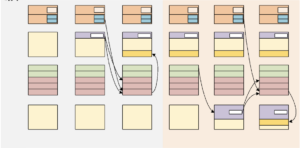
Figure 2. Secure Boot.
Secure Boot
Secure boot is a necessary design requirement for TEE SoC and is a prerequisite for ensuring system security. In the secure boot process, it is usually necessary to verify the authenticity and integrity of the code to ensure that the code has not been tampered with. The secure boot process designed in this work is shown in Figure 2. The dual-core boot process is divided into two phases: TEE CPU boot and REE CPU boot. The REE CPU is hung until the code is loaded and verified. The secure boot process of the TEE SoC is as follows.
- When the SoC is powered on and reset, the TEE CPU first runs the code in BootRom. The code is mainly responsible for loading the ZSBL code, and carrying the corresponding signature to the ZSBL RAM in the Isolated System through the secure serial port.
- The TEE CPU performs SHA-1 extraction digest of the loaded program in the ZSBL RAM and performs the decryption of the signature using the RSA public key of the ZSBL code segment inside the BootRom for signature verification of the loaded program. The TEE CPU jumps to ZSBL RAM to run when the verification is passed.
- ZSBL first configures the IOPMP restricted access address in the SoC. Then it starts the secure serial port to load the TEE_REE code and the code signature signed by the RSA private key. After the loading is completed, the TEE CPU computes the SHA-1 digest of the loaded code and data by using the Secure Core and verifies the signature using RSA before it starts to execute the TEE software stack.
- The TEE CPU performs SHA-1 on specific processes in the REE software stack to obtain the corresponding digest list, laying down the foundation for secure dual-core communication later. After completing the list generation, the TEE CPU will configure the REE CPU boot address and pull the reset signal of the REE CPU high to start the REE CPU. At this point, the secure boot of the TEE SoC is completed.
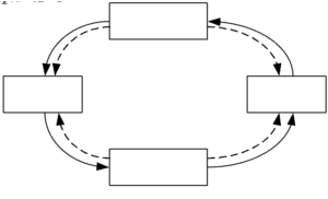
Figure 3. Mailbox-based dual-core communication.
Design of Mailbox
In a dual-core SoC architecture, inter-processor communication (IPC) is key to provide data communication, event control and resource sharing. As shown in Figure 3, we use mailbox communication based on shared memory combined with inter-core interrupts, while the shared memory is implemented using FIFO. The dual-core processes can transfer data through mailbox, i.e., read and write communication according to the mutually statutorily agreed interaction protocol. To solve the read/write consistency problem of the shared memory and protect the data security of the security core in the shared area, the TEE CPU and REE CPU use independent shared memory, respectively. The basic operation is following, as can be seen from Figure 3, when the REE CPU transfers data to the TEE CPU via mailbox, it first writes the data type, data length and data to the FIFO of mailbox, and when the write is completed, the R_Intr signal will be generated to inform the TEE CPU to receive the data from mailbox. When the TEE CPU finishes receiving the data, it generates the R_OK_Intr signal to inform the REE CPU that this communication is complete. Similarly, the transfer of data from TEE CPU to REE CPU is also done by the R_Intr and R_OK_Intr signals. Therefore, in order to implement dual-core communication, both processor cores need to add two mailbox interrupt responses.
Multi-level Access Policy
To secure the dual-core communication, we designed a multi-level access control strategy based on shared memory. The TEE CPU implements access control of the REE CPU based on the multi-level access control policy to protect the security of shared memory. Our TEE SoC provides three different security access control policies.
- Level 1: direct access policy, it does not require any access control, and the TEE CPU directly provides access services to the REE CPU, only requires the process to meet the protocol of dual-core communication.
- Level 2: integrity access policy, it authenticates the REE CPU process access to the security zone resources to ensure that the process code or data has not been maliciously tampered with.
- Level 3: confidentiality access policy, including validity and integrity access policy and data encryption policy, is used for access control of high-security data, such as access to keys, extraction of fingerprints, extraction or change of passwords, update of data in the security zone, etc.
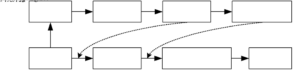
Figure 4. Confidential Access Flowchart.
We specify that the transaction requesting encryption is a confidential access event, as shown in Figure 4. For this type of access, it is first necessary to SHA1 the code block of the access task to obtain the corresponding digest and compare it with the task code digest obtained by secure boot to achieve integrity authentication. When the authentication is passed, the TEE CPU transmits the cipher text (using AES encryption) through the common shared memory in mailbox. At this time, if a malicious process intercepts the value read by mailbox, it is invalid. To transfer the key to REE CPU, we use the security registers and the TEE-only writable memory area in mailbox for the secure transfer. When REE CPU finishes receiving the cipher text, TEE CPU writes the encryption key to a separate block of memory (FIFO) in TEE, while the write security register is valid and writes an interrupt signal to inform REE CPU to read it. The interrupt handler of the REE CPU will first determine whether the value of the security register is valid, i.e., give the REE CPU permission to read the memory area in the mailbox that only the TEE CPU has write access. When it is valid, REE CPU reads the data from the isolated memory; otherwise, it reads from the shared memory. Therefore, for confidential access, the original access process returns the value as cipher text. When REE receives the cipher text, it invokes a specific key request task to obtain the AES key so that an attacker cannot easily obtain the key to decrypt the cipher text. In our approach, the AES key is not directly exposed to the REE. The confidentiality task is transmitted in two parts, the first part is the TEE sending the encrypted cipher text to the REE via the shared memory in the mailbox. The second part is that the REE requests the AES key from the TEE, which also verifies the integrity of the key request task, and to ensure security, the key is transferred through isolated memory.
In our work, A TEE-secure SoC system with a dual-core RISC-V CPU and a multi-level bus architecture. The newly proposed IOPMP of RISC-V is also utilized to restrict the access rights of CPUs in the non-secure environment. In order to improve the processing efficiency of secure boot and encryption and decryption operations, we designed hardware computing units for RSA, AES, and SHA1 algorithms and integrated them into the TEE SoC as a Secure Core; the accesses to the Secure Core is restricted by the IOPMP. At the same time, we designed a simple secure boot process based on the CoT to ensure the boot-time authenticity and integrity of the SoC environment boot. We use mailbox based on shared memory and inter-core interrupts to enable dual-core communication. Our architecture has lower resource consumption, higher flexibility, and better security, which well meets the basic security and computing requirements of IoT edge devices.