Jiacheng Yang, Yahui Teng, Bingquan Huang
Guangdong University of Technology
In the China Postgraduate IC Innovation Competition this August, T-Head sponsored the design challenge: Building the Dual-core TEE security solution based on Xuantie Open E902. In this competition, there are lots of excellent designs, and some of the teams take the initiative to share their designs. The team Reshaker has shared their design in TEE SoC Based on RISC-V. This is another team from Guangdong University of Technology, they won the second prize in the competition, they introduce their design in this blog.
Preface
Rapid development of IoT has engendered various information security issues. Trusted execution environment is an effective means to ensure security. In this article we will address the importance of building capability of TEE under RV processor to achieve such security.
Overall Solution
We will design a minimal SOC system with TEE support using E902 as the processor. To improve the security of the system, we start from the following aspects:
- The dual-core solution, comprised of secure and non-secure cores, shows achievement in physical isolation of the CPU. This is to ensure that non-secure cores have no access resources within the secure world, so that each core has its own independent memory area within it for running programs.
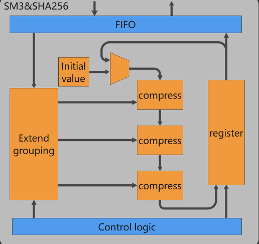
- Crypto encryption and decryption modules are implemented in hardware. The hardware is also where AES/SM4 algorithm is used to achieve fast data encryption and decryption. SM3/SHA256 is incorporated for data compression and integrity verification; RSA algorithm is utilized for signature verification. We strive to improve the security of hardware cryptographic algorithms through anti-attack design, while ensuring root security.
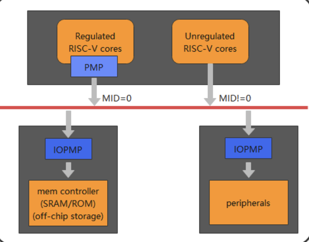
- Restrict the access of non-secure cores to resources within the secure world through IOPMP modules, such as Crypto encryption and decryption modules.
- Implement a secure boot process. Running a non-secure core only after the secure core has been configured with PMP registers, i.e., after restricting the non-secure core’s access to some resources.
In summary, the overall security solution is shown in Figure 2-1.
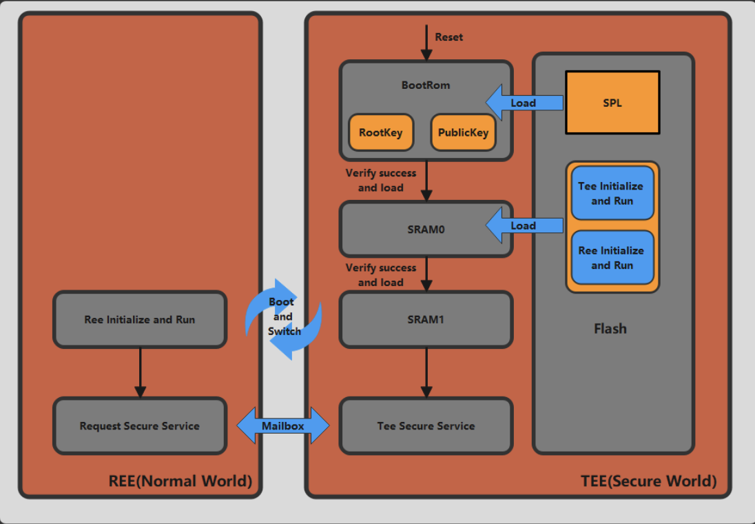
Figure 2-1 Secure boot process
1.We conduct necessary preliminary preparations before secure boot process.
(a) Randomly generate the RootKey required for SM4/AES algorithm encryption and the PublicKey required for RSA algorithm, and solidify them in the BootRom of the security core, while the private key of RSA is kept by the administrator; in addition, a small piece of code is solidified in the BootRom of the security core for power-on self-boot, and the main function is to carry SPL (Second Stage Program loader) in Flash and perform administrator authentication as well as data integrity verification, and after decryption is completed, it will be carried twice.
(b) All the program code stored in Flash is encrypted by SM4/AES algorithm RootKey used is the same as that in the secure core BootRom. In addition, the program stores the encrypted program, as well as the hash value processed by RSA.
(c) A small program is also solidified in the BootRom of the non-secure core for power-on self-boot. Its main function is to query the change of the Secure Configuration Register value.
2. The secure boot process is roughly divided into the following steps.
(a) When the secure core is powered on and reset, the chip will run from the starting address 0x00 in BootRom. Meanwhile, the secure core BootRom will access the Flash through the secure SPI serial port. It reads the signature, hash value and encrypted SPL program, while the non-secure core is also powered on and reset. the Secure Configuration Register value.
(b) As shown in Figure 2-2, the security core calls the Crypto encryption and decryption module. Firstly, it calls the RSA algorithm and uses the PublicKey solidified in the security core BootRom to verify the signature while obtaining the correct hash value. Secondly, it calls the SM3/SHA256 module to process the received SPL program. This will generate a new hash value. If the result is consistent, the identity verification and data integrity verification are passed. Last but not the least, if the identity verification and data integrity verification are passed, the SPL program is decrypted with AES/SM4 using the RootKey. RootKey and PublicKey are carried to SRAM0. The TEE security core running address also jumps to the valid code start entry of SRAM0.
(c) We introduce a code program for data carry in the SPL program. Similarly, the second stage of Bootloader will carry encrypted TEE initialization and Runtime, as well as Normal World’s REE initialization and Runtime, the signature, hash value. After passing the authentication and data integrity verification, the code program is decrypted and the TEE initialization and Runtime program is carried to SRAM1. While the REE initialization and Runtime program is carried to the storage area of Normal World, the TEE secure core running address first jumps to SRAM1 which belongs to the secure world. This process starts the security configuration of the TEE OS, i.e., configuring the PMP registers to restrict the non-secure core’s access to access to security resources.
(d) After the security core completes the security configuration, it writes a value to the Secure Configuration Register. Once the non-secure core queries the change in the value of this register, it jumps the non-secure core running address to the entry location of the REE initialization and Runtime, i.e., it starts running the non-secure world,,thus ensuring the start of the the non-secure core.
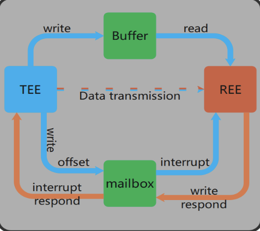
(e) Subsequently, the communication between REE and TEE is based on the Mailbox interrupt mechanism; the REE core will write data and instructions to shared memory, then trigger an interrupt and send the stored address information to the TEE core. TEE core will respond to the interrupt according to the request; If the response is successful, TEE core will get the data and instructions according to the accepted address information, and then process the data according to the type of instructions in response to the REE core.
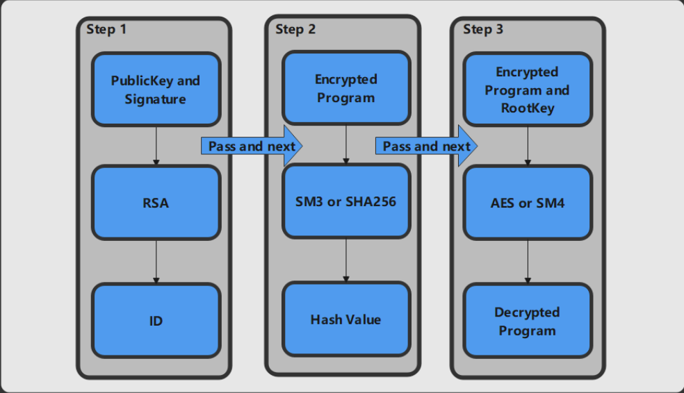
Figure 2-2 Security verification and decryption process
Building a hardware SOC system
The original Wujian 100 platform is shown in Figure 3-1.
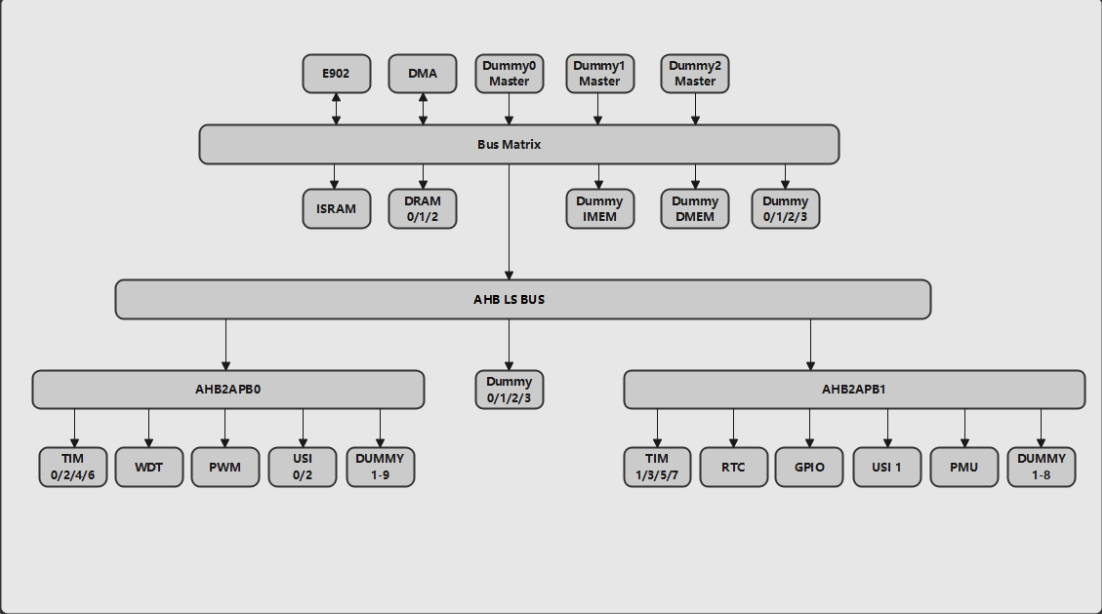
Figure 3-1 Wujian 100 SOC platform architecture
The final hardware SOC platform architecture is shown in Figure 3-2;
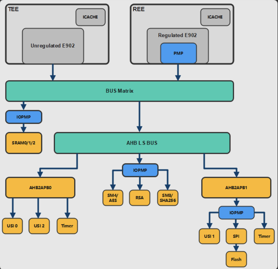
Figure 3-2 Dual-core TEE security SOC platform architecture
- Dual-core
In order to meet independency software programs, each core has been incorporated piece of storage area. The two CPUs are tightly coupled by cutting out the original ISRAM and adding an ICACHE inside each CPU, since ICACHE is directly connected to the instruction bus without passing through the bus matrix, the system can speed up the instruction transfer as well as faster CPU processing speed.
2. AES/SM4
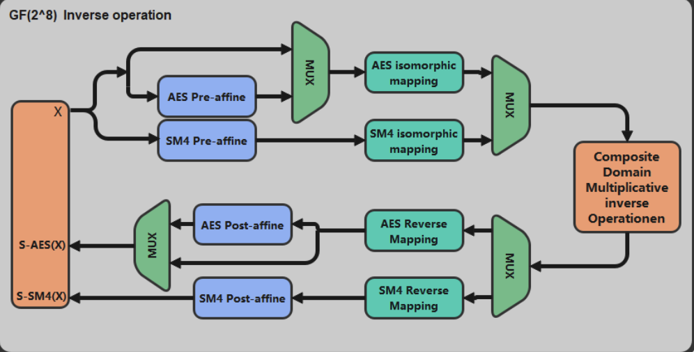
AES-128/192/256 and SM4 adopt key extension and wheel transformation parallel reconfigurable design, merging and integrating of four algorithm modes into one IP; the S-boxes of AES and SM4 are based on composite domain GF((2^2)^2)^2)^2) regular basis reconfigurable design, using reconfigurable S-boxes based on secret shared threshold, resisting side channel analysis attacks such as CPA, DPA and DFA, etc., design AES with SM4 based on random mask to resist power attack schemes, design error detection schemes for circuits based on error detection sub-modules, and optimize the design by combining reconfigurable ideas.
-
- Reconfigurable design of AES&SM4:
- Multiplexing of the interface layer in sequence: including input of bus data, allocation of control registers, storage of calculation results and output of operation status.
- Multiplexing of the control layer: all jump states can be combined into the same state, thus merging multiple state machines into one.
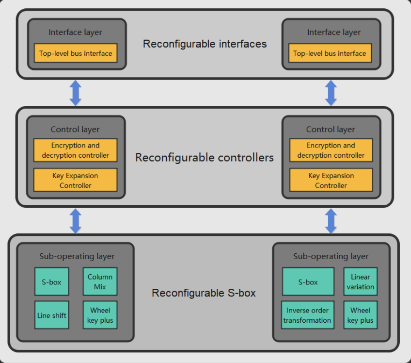
Figure 3-3(a) AES structure schematic Figure 3-3(b) SM4 structure schematic