Author: P R Sivakumar, Founder and CEO, Maven Silicon
LinkedIn Profile: https://www.linkedin.com/in/sivapr/
Every country realizes the importance of producing skilled chip designers who could decide their success as soldiers by creating advanced AI chips for winning the Chip War. Also, every country is now gearing up to build a good semiconductor manufacturing ecosystem to balance the global semiconductor supply chain that could overcome any more supply chain disruptions experienced during the pandemic. But the advanced foundries without next-gen chip designers would be the same as ‘Fabs without Chips’. So, in this article, I want to inspire the electrical and electronics engineers who can lead the semiconductor industry as the next generation of chip designers, sharing my insights and explaining how ‘Semiconductor rules the world’. Also, I hope this article inspires the VLSI Design companies to upskill and support their chip design workforce for their long-term VLSI career development, prioritizing and investing in their Learning and Development initiatives.
1.Chip War
The geopolitical AI cold war between the US and China is perceived as Chip War. Artificial Intelligence technology is one of the essential technologies for any country to emerge as the most powerful country with its next generation of defense and space technologies. Chip war is all about fighting for their dominance in AI.
The AI systems can be trained on vast data centers built with cutting-edge AI chips. So, every country is funding and collaborating with global chip manufacturing companies to build advanced fabs for their future.
The advancement and implementation of AI technology rely on semiconductors, and it demands semiconductor architectural improvements. The improvements in chip design for AI will be less about improving overall performance and more about speeding the movement of data in and out of memory with increased power and more efficient memory systems.
Only with higher technology nodes we can fabricate complex SoCs as cutting-edge AI chips that integrate complex neural engines and memories using new technologies like Chiplets. So, every country is gearing up with advanced fabs.
2.Chip Industry
Our journey in the semiconductor industry started with making IC with four transistors, and it’s continuing to produce complex SoCs with 100s of billions of transistors.
2.1 History:
Defense has been a key driver for the evolution of the semiconductor industry. Defense departments & institutes, especially DARPA in the US, funded inventing chip technologies and introduced the concept of using chips to create advanced defense technologies like next-gen missile guiding systems.
The first monolithic IC was invented by Robert Noyce at Fairchild Semiconductor. In 1960 first operational IC was created at Fairchild. Later the chip manufacturing ecosystem was built with a supply chain[Machines and materials] spread across Taiwan, Netherlands, South Korea, Japan, and other countries, beyond the US. The chip industry emerged from Texas, Silicon Valley, and expanded into other countries like Taiwan, as a global industry. Today more than 90% of the advanced chips are manufactured in Taiwan, mainly by top foundries like TSMC. Chris Miller’s book ‘Chip War’ can walk you through the incredible journey and evolution of the chip industry.
2.2 Semiconductor Ecosystem:
The global semiconductor industry is generating yearly revenue of 500+ billion USDs and growing exponentially towards generating 1 trillion USD by 2030. In my view, it reflects the evolution of VLSI technology. In terms of technology, we are making SoCs with 100+ billion transistors and evolving towards making chips with 1 trillion transistors by 2030.
2.3 Inventions and Innovations:
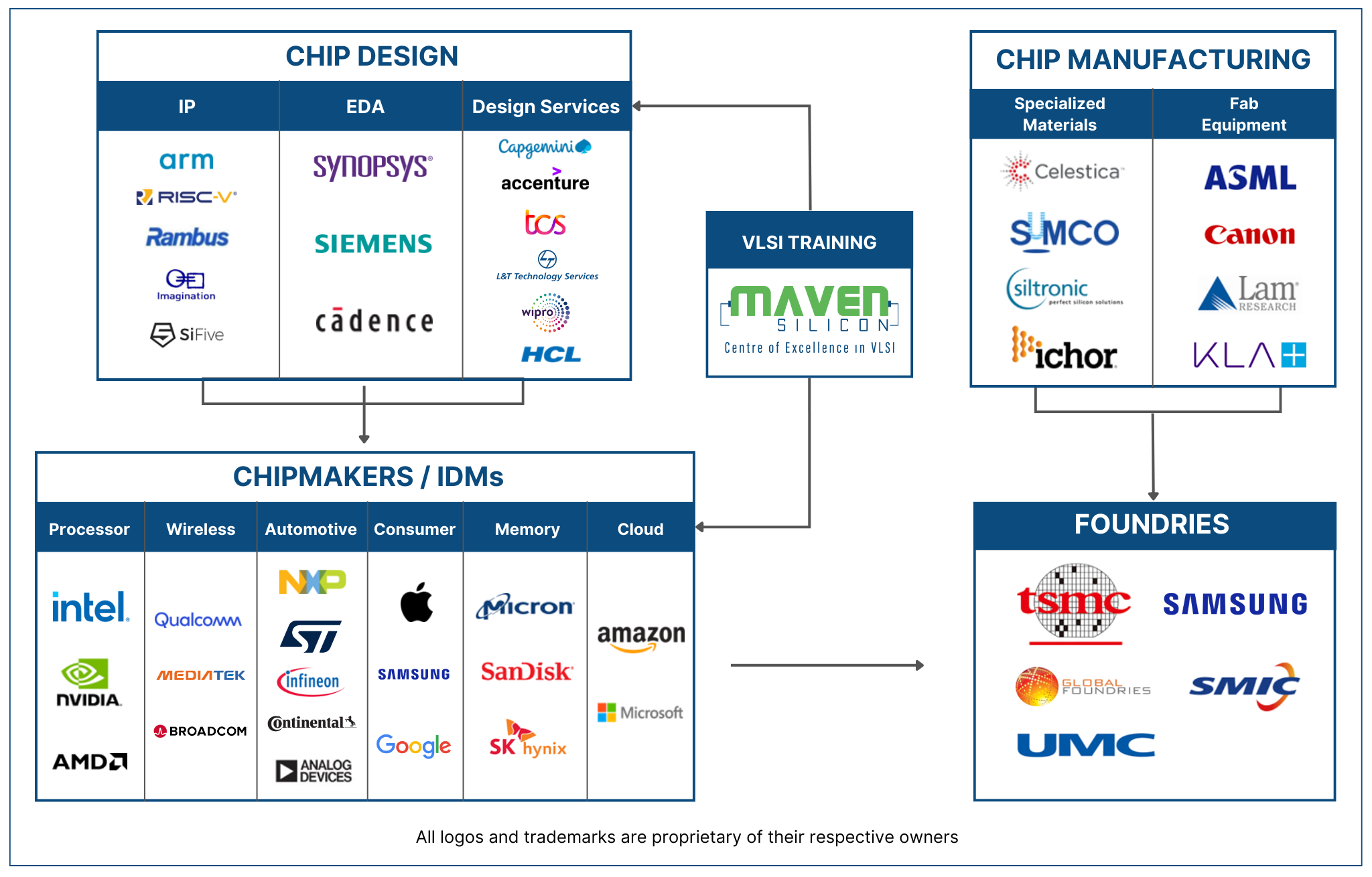
The semiconductor ecosystem incorporates various players like OEMs, IDMs, Fabless-IP, EDA, and Foundries. The ecosystem is evolving with all the inventions and innovations by its players/stakeholders. Every stakeholder contributes equally to the growth of the global semiconductor industry, and some of the highlights I am listing here for your reference.

Semiconductor Ecosystem | OEM-Original Equipment Manufacturers, IDM-Integrated Device Manufacturers, IP-Intellectual Property, EDA-Electronic Design Automation
OEM: Apple is adopting a smartphone-design approach for their MacBooks. Its M-series SoCs are now built with ARM RISC processors using 5 nm technology, replacing the popular desktop CISC processor, and the complexity ranges from 16 billion to 100 billion transistors.
IDM: Intel is growing its foundry business with the vision of creating an open system foundry to empower the chipmakers to create a System of Chips[SoC] using various technologies like 2.5D&3D advanced packaging, Chiplets with Universal Chiplet Interface UCIe, and System Software solutions.
Fabless-IP/Chip: ARM is still ruling the semiconductor industry as the most successful IP company, with the credit of having hundreds of billions of electronic devices shipped with ARM cores. World’s fastest supercomputer Fugaku built with more than 7 million ARM cores, is one of the highlights beyond its dominance in the smartphones, IoT, and Automotive market segments.
RISC-V open ISA began its journey of open era of computing from the CPU graveyard, where we witnessed the burial of many proprietary specialized ISAs. Now RISC-V is emerging as an industry standard open ISA for all kinds of processors, general purpose and specialized processors. Esperanto, SiFive, Western Digital, Alibaba, and many more have been creating new powerful processors and cutting-edge AI Chips with RISC-V open ISA and empowering the semiconductor ecosystem.
Nvidia and AMD continue to rule the global semiconductor industry as fabless chipmakers with their next-gen state-of-the-art GPUs and CPUs.
EDA: EDA is acquiring intelligence using AI technologies to help designers achieve optimal PPA results. Synopsys has recently released Synopsys.ai as the first full-stack AI-driven EDA suite for chipmakers, following its successful DSO.ai for Design Space Optimization. EDA on the cloud similar to SaaS and Multi-die-system solutions are some of the other innovative EDA solutions from the EDA industry.
Foundry: Intel is expanding its foundry business with its open system foundry vision for advanced fabrication. TSMC is also expanding its foundry business in the US beyond Taiwan. Other players like Samsung and Micron are also investing heavily in building new foundries with advanced fabrication technology. Following the US Chips Act funding, every other country well known for semiconductor design, including India, is investing heavily in this fabrication space towards becoming self-reliant.
2.4 Investments:
The US introduced Chips ACT funding with USD 280 billion to boost semiconductor R&D and manufacturing in the USA. Currently, the US is producing only 10% of the chips made globally and aims to achieve 30% by 2030.
India introduced USD 10 billion incentive package for building a semiconductor chip manufacturing ecosystem in India. Foxconn and Vedanta seek to bring European chipmaker ST Microelectronics as their technology partner in their proposed India manufacturing unit. ISMC (US$3 billion investment) and Singapore-based IGSS (investment worth INR 256 billion) will set up semiconductor plants in Karnataka and Tamil Nadu, respectively.
2.5 Opportunities:
As per the Deloitte report, 2 million direct employees run the global Semiconductor Industry, and this fast-growing industry needs additional 1 million workers by 2030.
India has a very fast-growing electronics system design manufacturing (ESDM) industry. According to the Department of Electronics and Information Technology, nearly 2,000 chips are being designed annually in India. More than 20,000 VLSI engineers are working on various chip design and verification aspects.
Semiconductor Fab units require huge investments, gallons of water for production, uninterrupted electricity supply, high operating costs, and frequent technology replacement. This is why India’s contribution to the global semiconductor industry has focused on its technical competencies in R&D, design, etc., due to its talent pool in IT design and R&D engineers.
Academia with 2500+ engineering colleges produces 1.5 million engineers in India. Only 2.5 lakh engineers succeed in getting jobs in the IT sector. Excluding the IT software services, only 50000 engineers enter into the core industry, including all the domains. The number of engineers directly enter into the Indian Semiconductor Industry could be in the range of 5000 to 10000, which is insufficient. So, we at Maven Silicon bridge the gap between academia and the semiconductor industry, collaborating with our industry partners and academia in India. Also, Maven Silicon emerged as a VLSI Centre of Excellence[VLSI-COE] for the global semiconductor industry, upskilling the workforce[experienced VLSI engineers] worldwide using our corporate VLSI training solutions.
3. Summary
Software giants Amazon, Microsoft, Google, and Facebook are now building their chip design centers and making their chips for their data centers. The emerging technologies AI, 5G, Cloud, IoT, and Automotive demand more advanced chips and accelerate the semiconductor industry’s growth further. So the global semiconductor industry needs millions of skilled VLSI engineers to meet this growing demand and emerge as a trillion-dollar industry by 2030.
It’s very evident from history that the semiconductor industry rules the world beyond wars. Robert Noyce, Jack Kilby, Gordon Moore, Morris Chang, and many more great engineers and entrepreneurs ruled this semiconductor industry with their inventions and innovations and built the semiconductor ecosystem as architects. As a curious electrical engineer reading this article, you could be the next one continuing this incredible journey as our hope.


