

By Bob Wheeler, Principal Analyst, The Linley Group
Chiplet-based designs promise reduced development costs and faster time to market, but they’ve been exclusive to large chip vendors. Now, the industry is building an ecosystem intended to enable designs combining third-party chiplets that employ different process nodes. At the same time, RISC-V is enabling greater CPU innovation through its open-source model. These trends create an opportunity for a RISC-V chiplet vendor. Ventana Micro Systems sponsored the creation of this white paper, but the opinions and analysis are those of the author.
The Post-Moore Era
The days of one-size-fits-all processor architecture are gone, as the slowdown in Moore’s Law forces engineers to optimize their designs for domain-specific workloads. Although this trend is most pronounced in AI processors, designers have also been forced to optimize processors for other applications owing to diverging power constraints and performance requirements. These segments include data-center infrastructure, where microservices-based software and scientific computing, for example, differ widely in their compute requirements. Service-provider infrastructure, including the 5G radio access network, prioritizes efficient and secure data movement with tight thermal budgets. Automotive and autonomous-vehicle applications are similarly constrained by power and space combined with real-time processing of sensor data.
As design costs for leading-edge SoCs rise, developing monolithic workload-optimized processors becomes cost prohibitive for all but the largest vendors. To offset rising development costs and improve manufacturing yield, some vendors began using several small die, or chiplets, rather than one monolithic die. AMD employs chiplets in both its desktop-PC and server processors; Intel and Marvell have also released chiplet-based products. Nearly every such design, however, uses chiplets designed exclusively in house. This situation limits chiplet adoption to companies possessing the resources to design complete processors.
Ventana Micro Systems is among the companies working to democratize chiplet-based design by creating a third-party ecosystem. It’s developing a RISC-V compute chiplet in leading-edge process technology that customers can use to create custom processors. Providing a high-performance compute die allows customers to focus on adding workload-specific value while lowering their engineering costs and reducing time to market. Customer examples could include data-processing units (DPUs), storage processors, and AI accelerators. Further democratizing processor design, Ventana chose the open and extensible RISC-V instruction set, removing licensing barriers and promoting open innovation.
Chiplets Power Leading Processors
Over the last several years, chiplet-based design gained rapid adoption at large vendors including AMD, Intel, and Marvell. AMD has now shipped three generations of PC and server processors using its chiplet approach, which employs a low-cost organic substrate. By instantiating eight cores per compute die (CCD), it can build processors ranging from 8 to 64 cores (in the current generation). The CCD includes CPUs, cache memory, and a fabric interface, whereas an I/O chiplet provides all external interfaces such as PCI Express, DDR4 channels, socket-level interconnects, and other I/O. This division allows AMD to use leading-edge technology for the CCD—7nm for the Zen 3 generation—and trailing 14nm technology for the I/O chiplet.
Intel first employed chiplets in FPGAs, but it’s now expanding their use across server processors, PC processors, and GPUs. The company’s next-generation Xeon processor, code named Sapphire Rapids, uses chiplets to exceed the reticle limit imposed by a monolithic design. Compared with AMD, Intel uses coarser division that marries CPUs, cache, and I/O on a chiplet then scales at the package level using four of those chiplets. It uses a proprietary silicon-bridge technology (EMIB) to connect the die, adding both cost and performance relative to an organic substrate. In its forthcoming GPU (Ponte Vecchio) for high-performance computing, the company employs both EMIB and 3D stacking to combine a massive 28 logic die in a single package.
The slowdown in Moore’s Law is driving increasing adoption of chiplet-based designs, as evidenced by Intel’s Meteor Lake PC processor for 2023. New process nodes continue to increase transistor density, but increasing wafer costs result in little or no reduction in the cost per transistor. Each new node is producing smaller speed increases and power reductions as well. Chiplets provide an alternative to monolithic designs, enabling greater transistor counts while eliminating the requirement to use same process for all functions. Chip designers are no longer forced to redesign I/O blocks or other functions that don’t benefit from the latest node. Chiplet-based design can also ease verification, which is a major source of schedule risk in complex monolithic designs.
Democratizing chiplet-based design, however, requires standardizing die-to-die (D2D) interconnects so that multiple customers may integrate a third-party chiplet. Otherwise, each chiplet remains customer-specific, reducing the economic advantage of disaggregating the design. The earliest work on die-to-die interface standards came from the networking world, but serial (serdes) interfaces increase design complexity, latency, and power for interconnects that are natively parallel such as AXI, CHI, or TileLink. Intel developed a parallel interface for its EMIB, and it later published the Advanced Interface Bus (AIB) specification and RTL on GitHub under a permissive open-source license. AIB 1.0, however, doesn’t support lower-cost organic substrates.
Adopted as a subproject by the Open Compute Project in 2019, the Open Domain Specific Architecture (ODSA) workgroup developed a parallel die-to-die interface suitable for both organic substrates and silicon interposers/bridges. Like AIB, ODSA’s Bunch of Wires (BoW) PHY specifies single-ended DDR data signals with a forwarded clock, minimizing complexity, power, and latency. As Figure 1 shows, BoW can serve as the PHY layer for both on-die buses and off-package interfaces. Coherent die-to-die connections, however, also require link-layer compatibility.
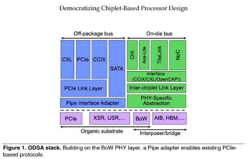
In addition to the BoW interface, ODSA has workgroups developing BoW test requirements, a link layer, proof-of-concept prototypes, a format for chiplet physical descriptions, and chiplet business workflows. By creating interfaces, reference designs, and workflows, ODSA is laying the groundwork for an open chiplet marketplace that will enable chip vendors to source interoperable chiplets from multiple suppliers.
From General Purpose to Domain Specific
Whereas x86 server processors once dominated data-center-silicon shipments, the trend toward disaggregation is driving a greater diversity of chips. A new category, DPUs are used in smart NICs as well as security and storage appliances, offloading network processing from the host. Storage processors can replace x86 processors in all-flash arrays, terminating network traffic and providing fanout to NVMe SSDs. The explosion of AI created multiple chip types, including inference accelerators and training chips that may operate as standalone processors. Cloud data-center operators are developing their own server processors in addition to these specialized designs. They see the need for a chiplet ecosystem to accelerate time to market, reduce the cost of large chips, and reduce dependency on leading-edge fabrication. Alibaba, Facebook, Google, and Microsoft collectively deliver this view through the ODSA End User workgroup.
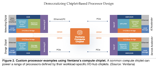
Figure 2 shows example processor designs that customers can build using a chiplet approach, all using a common compute chiplet. The I/O-hub chiplet implements only the I/Os, DRAM interfaces, and hardware blocks required for the target application, reducing total silicon area and improving performance per watt compared with a superset design. Processors that require a large hardware accelerator, such as a neural network engine, can employ multiple chiplets, separating this dense logic from the I/Os. This chip-level disaggregation enables reuse of common I/Os and optimal process technology selection for each chiplet.
Hyperscale data-center operators consume many chips and some develop SoCs, but they lack the design resources to develop high-performance out-of-order CPU cores. Some of these operators use an ASIC design flow to outsource much of the development, but monolithic ASICs still suffer from lengthy development cycles. A marketplace of proven chiplets could reduce development time, cost, and risk. Some incumbent chip suppliers may view an open chiplet ecosystem as a threat, but a number of startups are embracing the new business model.
Disaggregating the RISC-V Processor
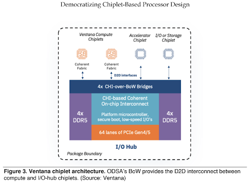
As Figure 3 shows, Ventana’s processor design includes a standard compute chiplet and a customer-defined I/O-hub chiplet. The company’s initial compute chiplet is a 16-core RISC-V design built in 5nm process technology. Ventana is designing an aggressive out of-order CPU that it expects will offer single-thread performance rivaling that of contemporary Arm and x86 cores. The compute chiplet will have an ODSA BoW interface to connect with the I/O hub. The company is developing link and transaction layers that will present Amba CHI (Coherent Hub Interface) and AXI interfaces to the I/O-hub’s blocks.
The I/O hub can integrate multiple BoW interfaces to connect compute chiplets, enabling processors with 128 or more cores. Customers can also connect proprietary or third-party accelerator chiplets to the I/O hub, which provides a coherent interconnect across compute and accelerator chiplets. The I/O hub also integrates system I/Os such as DRAM interfaces, PCIe ports, or Ethernet ports, which the compute chiplet lacks. Because the I/O hub typically omits dense logic and memory, it can use mature technology such as 12/16nm.
Once Ventana has proven its compute chiplet and can supply known-good die (KGD), customers need only purchase or develop an I/O-hub chiplet to complete the processor design. The chiplet approach reduces the customer’s tape-out costs, as the I/O hub can use an older process. It also means customers needn’t license and integrate CPU IP, reducing non-recurring expenses and verification work. Many of the I/O-hub functions are available as off-the-shelf IP, reducing design time.
Conclusion
Over the past several years, chiplets have moved from a buzzword to a proven technology, enabling chip shipments in the millions of units per year. Lacking a mature ecosystem, however, chiplet-based design has been available to only large vendors. Now, the industry is poised for broader adoption once D2D interfaces are standardized and a wave of vendors adopt new chiplet-based business models. Customer demand is creating momentum behind this approach, with the ultimate goal of rapid chip design using mix-and-match third-party chiplets.
The chiplet approach reduces the cost and time required to develop custom processors. By using an off-the-shelf compute die, customers can focus on developing the IP that differentiates their processor for a target application rather than duplicating a common block. Most of the I/O-hub functions are readily available as IP blocks, so the customer task is primarily integration. Using a compute chiplet also allows customers to use leading-edge process technology for that function, whereas many SoCs lack the volume to justify a monolithic design in that same node.